
news
A charger worth the price
Have you heard of a newly emerging consumer trend called “convenium?” A portmanteau of “convenience” and “premium,” it refers to consumers’ willingness to pay a premium for products or services that offer more convenience. This trend has been particularly noticeable in the consumer electronics market, where users are more likely to choose expensive alternatives that save them time and effort. A good example is electronic chargers. Whereas customers were formerly satisfied just by a small blinking “charging” lamp, consumers today pay extra money for a lighter and faster charger. Gallium nitride (GaN)-based chargers command a premium price over traditional silicon-based versions; nonetheless, they are becoming increasingly popular owing to their advantages, including reduced heat generation, compact and lightweight body, and fast charging speed. In other words, such chargers are worth the higher cost because of their higher efficiency.
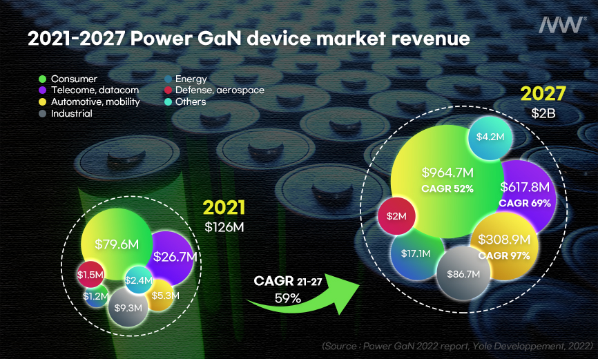
In this light, the market size for GaN-based power semiconductors has rapidly increased, driven by the growing demand for consumer electronic chargers. In 2020, Xiaomi launched 65 W GaN chargers for its laptops; these boast a 48% reduction in size compared to that of the previous model. In 2021, Apple introduced its first 140 W GaN high-speed charger for the 16-inch MacBook Pro. GaN technology has been widely adopted in various industries, including aerospace and satellite wireless communication, data transmission, electric vehicle (EV) charging, and solar energy. The global market size for GaN based devices is projected to reach approximately $2 billion by 2027; this represents a 15-fold increase from the estimated market size of $126 million in 2025. Though the ongoing discussion over the use of GaN for EV onboard charging and 5G data communication indicates that the auto and telco industries have the highest growth potential, consumer electronics, including GaN chargers, have actually driven market growth from the beginning. Specifically, some chargers are worth more money (Power GaN 2022 report, Yole Development, 2022).
Born with a silver spoon in the mouth? The reasons for expensiveness
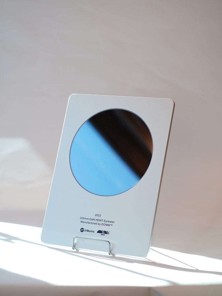
The reason for highlighting the premium price above is that cost pressure has been the biggest challenge in manufacturing. One significant contributor to the cost is the epiwafer, a key material in GaN-based devices, including GaN high electron mobility transistors (HEMTs), that can account for up to 40% of the total cost. The epiwafer is produced through the critical process of epitaxy, in which a thin GaN layer is grown on top of a single crystal substrate, such as Si or silicon carbide (SiC). The epitaxy process is considered the key determinant of the performance and reliability of GaN semiconductors.
Currently, one important question is how to achieve the economy of wafer size, where larger wafers can produce more semiconductor chips per batch, thus making the manufacturing process more economical. GaN-based devices typically use 6-inch (GaN on Si) wafers, and the silicon industry commonly uses 8- and 12-inch wafers. This is because the epitaxy process required for GaN devices is more expensive, and technical limitations exist in producing substrate wafers. Even if these issues were to be resolved, the cost of producing large GaN wafers would remain high owing to the cost of the utilities required for growth, need for high levels of reproducibility, and process environment required for device fabrication. Other complications include the need for a controlled and specialized manufacturing environment and proper handling and storage procedures for the GaN devices.
Multiple factors are interrelated in determining the cost competitiveness and productivity of GaN epiwafers. Generally, thicker GaN layers (thickness > 5 μm) can reduce the defect density; however, they can also hamper productivity owing to the increased growth time and increased costs from more frequent equipment maintenance. Another dilemma is that thicker GaN layers may lead to decreased yield owing to cracking defects, and using thicker substrates (thickness > 1 mm) increases the material cost. Therefore, an optimal fabrication process is required to reduce defects while maintaining thin GaN layers.
Who is destined to be the king of the GaN epiwafer market?
Considering the abovementioned technical difficulties, only a handful of manufacturers worldwide can provide commercial GaN epiwafers. Though many companies have established GaN business units in an effort to capture the market opportunities in next-generation chips, they will likely require a significant amount of time to produce commercially viable products.

Different companies adopt different business models in the market. Some integrated device manufacturers (IDMs) have come up with an end-to-end model from epiwafers to GaN-based chips since the early days of the market. For instance, Texas Instruments (TI), a global semiconductor giant, started product development in 2010 to build its capability in managing the entire processes for epiwafers and chips, including fabrication, assembly, and testing. Other IDMs focus on chip design and wafer manufacturing while outsourcing the product testing process. Given that the market for this new and versatile product is still in its early stages, with a size far from reaching the magnitude of hundreds of billions of USD, and that GaN-based products are approximately 50% more expensive than Si-based ones, IDMs with diverse business portfolios are reluctant to invest all of their resources in process optimization for the GaN business, which may take years to reach full growth.
While improved competitiveness for GaN requires the optimization of each process and reduction in costs, most IDMs struggle with the cost structure of epitaxial wafers as they account for the largest share of the cost price. This incentivizes them to buy commercially viable epiwafers from GaN epiwafer specialists, who are aiming for a market transition to GaN-based devices. This practice of outsourcing epiwafers has opened the gate for the market of GaN epihouse business, which in turn has driven down chip prices and accelerated market growth.
IVWorks is the only company capable of fabricating and selling GaN epiwafers in South Korea. It has had virtually no presence in the compound semiconductor segment. It has successfully developed its differentiated solutions for epiwafers, including proprietary AI, equipment technology, and intellectual property (IP) on semiconductor defect reduction, to enhance productivity and price competitiveness. As one of the industry-leading GaN epi-specialists, it provides general-purpose GaN epiwafers, covering both power and RF applications. IVWorks also offers full customization services for diverse customer needs, and it can thus position itself as an ideal partner for IDMs or foundry companies adding GaN products to their portfolios. Ever since the opening of the epihouse market, the Korean epi-specialist has continued its quest for new business opportunities by diversifying its business models, including B2B business for direct supply, joint development (JD) with global leading chip makers, and original design manufacturer (ODM) for new customer development. Industry experts highly appreciate its potential to be a game-changer, citing the company’s core technologies that can further strengthen its competitiveness in large-size wafer and mass production.
For a product like GaN-based chips, owing to the challenge of price pressure despite proven performance, R&D-driven technological competitiveness is the only long-term solution to accelerated market growth and wider adoption of GaN-based devices. Being the first mover will be a key leverage point in this promising market in the future.
Yoon-Seo Cho l Marketing Assistant at IVWorks
※This article reflects the subjective opinions of the contributor and may differ from the official position of IVWorks