
news
The era of constant everyday content generation is here.
Innumerable amounts of data are constantly transmitted using radio technology. Unlike other types of waves that require a physical medium for transmission, radio waves can spread even through the vacuum of space. So, what about in Earth? This is where all Digital devices communicate wirelessly. RF technology generally involves a radio system that uses an analog signal processing unit to send and receive electromagnetic signals through various amplification or filtering processes. Originally, RF was a concept that included both low and high frequencies. However, as communication frequencies increased from hundreds of MHz to several GHz, it also considered to meaning the development of equipment for high frequencies.

Amplifiers are used to significantly widen signals. Radio signals undergo more severe attenuation and noise than wired communication as they are transmitted and received through the air. This issue is mitigated by significantly amplifying the signals during transmission and reception. Therefore, amplifiers play a crucial role in the RF field.
An RF transmitter must emit signals with the maximum power to ensure their successful transmission to the desired location. Accordingly, an appropriate level of power amplification (PA) should be considered when sending radio signals. Conversely, the receiver must interpret information from initially weak and noisy signals as they have traveled a long distance. Therefore, low noise amplification (LNA) needs to be considered. In other words, PA and LNA are the core elements of RF amplification. An RF transistor duplicates and magnifies the change pattern in input and output currents. When the input signals are slightly wavy, the output follows the signals several dozen times while maintaining their content.
Silicon-based laterally-diffused metal-oxide semiconductor (LDMOS) transistors and high electron mobility transistors (HEMTs) based on III-V compound semiconductors such as gallium arsenide(GaAs) and gallium nitride(GaN) are mainly applied to semiconductor RF power amplifiers. GaN HEMT devices are produced by growing a GaN channel layer on a silicon carbide (SiC), gallium nitride (GaN), or silicon (Si) substrate. Unlike the other two compounds, GaN features a wide band gap and high-temperature stability. *When used as a power amplifier for a mobile communication network base station, the power density of GaN is 10 times higher than that of Si LDMOS. When used in radar and satellite transceiver modules, its power density is 8 times higher than that of a GaAs power amplifier, and its efficiency is 20% higher. These properties can contribute to weight reduction and energy conservation of the payload.
*ETRI, 2012 Eelctronics and Telecommunications Trends / Next Generation Energy Efficient Semiconductors : Status of R&D of GaN Power Devices
According to the <Active and Passive Systems for Telecom Infrastructure 2019 Report> released by Yole Developpement, a French market research institute, the GaN HEMT was projected to account for approximately 20% of the RF infrastructure market by 2025, a +12% increase in CAGR from the $239M figure obtained in 2018 and the highest growth among the top three groups, comprising LDMOS, GaAs, and pHEMT.

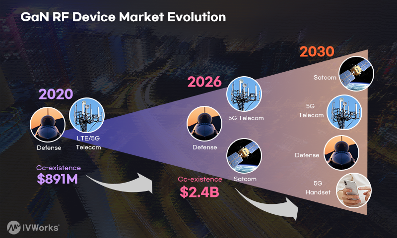
The size of the GaN power device industry is reportedly determined by changes in mobile communication services, military communication equipment, and threats to international security. The GaN RF device market, worth $891M in 2020, is expected to reach a whopping $2.4B in 2026 at a CAGR of +18%. Notably, defense and telecom infrastructure account for approximately 90% of said market, and the rapidly increasing popularity of 5G handsets is also significant. GaN RF devices offer widespread applicability in air defense, aircraft, weapon search, ships, weather services, mobile communication, and broadcasting of the L-, S-, X-, Ku-, and Ka-bands. X-band GaN power amplifiers are widely used in high-resolution radar transmitters, such as those employed in marine navigation. Ku-band GaN power amplifiers are applied to transmitters for guided weapon searches, aircraft radars, maritime radars, and terrestrial transmitters for satellite communication.
The GaN RF field has begun to draw more attention with the launch of 5G mobile communication services. 5G was launched to increase interconnectivity and trigger digital innovation in the industry beyond the limits of mobile communication, which was limited to voice and data, with ultra-high speed, ultra-low latency, and hyper-connection as its core elements. However, because the 5G frequency band is limited to sub-6 GHz and the mmWave band cannot be used, access to true 5G remains limited in South Korea.
As frequency is directly proportional to speed, a wide frequency range is required to transmit large quantities of data immediately, akin to the principle that an 8-lane road is less congested than a 2-lane road. However, securing a new frequency is difficult because most frequencies have been allocated to airplanes, the military, and broadcasting. Then, why we don’t use the new? Because the new mmWave frequency exhibits poor characteristics. Generally, low-band frequencies are low-capacity but offer good diffraction. As low-band frequency waves bend when encountering obstacles such as trees or buildings, their transmission range is wide. In contrast, high-bandwidth frequencies can transmit large amounts of information quickly but are significantly affected by obstacles. Considering attenuation due to moisture is also significant, communication quality also deteriorates during inclement weather, thus facilitating the need for constructing many base stations.
With mobile devices becoming more versatile, they require increasingly more network traffic, which may lead to data congestion. With the development of the Internet of Things (IoT), interconnected fields such as energy and transportation will require faster data transmission. The generational characteristics created by the popularization of over-the-top media services and non-face-to-face culture also contribute to the increase in the demand for mmWave. A larger capacity with a higher bandwidth must therefore be provided, increasing the physical costs associated with 5G services because base stations must be installed in various places to secure widespread coverage. In addition, to enable 5G connections in more applications in the same frequency band, the antenna must also be dense because electromagnetic waves must be spatially divided within one base station cell. Furthermore, additional processing power is required for 5G services to surpass existing networks.
As a result of these factors, there is a growing demand from the industry to increase power density to provide more power within the same footprint, which is possible by increasing the efficiency of the power conversion stage. When SMD packaging is used for existing Si-based power semiconductors, both power density and thermal density increase. Therefore, switching efficiency must be increased to eliminate the operating temperature limits of devices.
This situation is where GaN comes into play. GaN is more physically durable than Si, making it an ideal material for high-power switching at high frequencies. The low on-resistance and low switching losses allow the power converter to operate at higher switching frequencies. Thus, the size of the magnetic element required for the switching power supply is also reduced, thereby decreasing the overall solution size. Component manufacturers are faced with the need to meet the rising power demand by increasing power efficiency, which is a burden on existing infrastructure. Therefore, GaN is a promising material for the necessary power conversions associated with 5G network infrastructure.
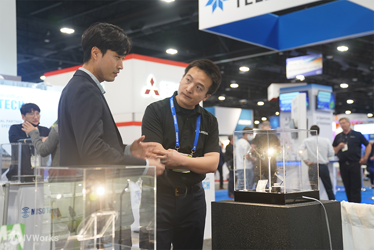
The International Microwave Symposium (IMS), one of the largest events in the field of radio frequency, was held in Colorado in June of this year. The IMS serves as a business arena for finding novel RF solutions. Over 6,000 registrants, and more than 400 exhibitors, participated for three days, demonstrating the massive scale of the industry. Many people visit this event for passionate technical discussions and review the latest issues faced by competitors. Accordingly, IVWorks also participated in the IMS, met with various engineers, and joined business and technical discussions.
IVWorks is the only GaN epi-house company in South Korea that provides products to foundries and IDM companies that outsource the production of GaN HEMT devices. As these products can be flexibly used in AI, In, and other fields while offering simple doping control, IVWorks can grow various layers to perfectly customize services. Two years ago, the company announced the success of large-diameter GaN on SiC, showing more than twice the chip production efficiency compared to its 4-inch counterpart. The IMS event in question featured widespread exhibits of RF devices such as APs, diodes, switches, capacitors, signal analyzers, generators, and die bonders. Many people expressed interest in the IVWorks exhibit, which introduced a relatively scarce material business.
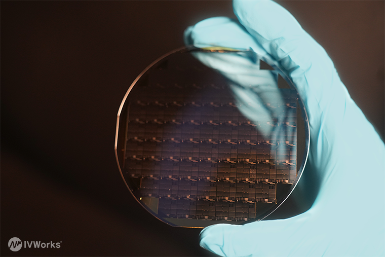
In particular, many visitors asked questions regarding the N+-GaN regrowth epiwafer, which was displayed offline for the first time. The N+-GaN regrowth, generated on an epitaxial surface grown by an MBE machine, can further maximize the efficiency of the final product. It enables manufacturing by specifying an area to be regrown and applies to 100–200 mm Si and SiC substrates. It also features a high doping concentration (n=5.0e19~1.0e20/cm3) and excellent side-wall contact characteristics.
In the RF power device field, GaN devices have already occupied a certain market share, which is expected to grow with the increasing prevalence of 5G. In contrast, the GaN DC power device market has only recently emerged. IVWorks has already completed the proactive development of large-diameter GaN on SiC as a response to rapidly changing market trends and is currently stimulating R&D to automate its AI platform <DOMM™> Lv. 4. Consequently, IVWorks is acquiring customers in the defense and telecommunication markets based on production technology that sets it apart from competitors.

The war of industries around the globe never stops. As long as industrial development continues, interest in the specifications and power efficiency of RF components will not end. News about emerging companies and business units to gain market advantages and investments in materials also never stops. In particular, the importance of GaN is being highlighted as 5G is taking deep roots in the industry. Indeed, what is the limit of GaN spreading throughout the industry through 5G?
Yoon-Seo Cho l Marketing Assistant at IVWorks
※This article reflects the subjective opinions of the contributor and may differ from the official position of IVWorks
Reference
ETRI, 차세대 GaN 고주파 고출력 전력증폭기 기술동향 (2014, 한국전자통신연구원)
ETRI, 5G 이동통신을 위한 GaN RF 전자소자 및 집적회로 기술 동향 (2021, 한국전자통신연구원)
동아사이언스, [세상을 바꿀 5G 이야기] ② 1초에 2GB씩 주고받는 밀리미터 웨이브 (2018.04.09)