
The place where compound
semiconductors are started

Products
DC Power GaN Epiwafer
DC-DC Converter, AC/DC Converter & Inverter, Switch, Field Effect Transistor etc.
Up to 300mm
GaN on Si
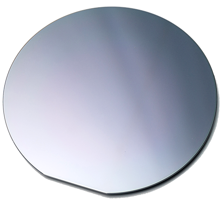
Up to 200mm
GaN on Si
GaN on Si Applications
EV/HEV
Data Server
Wireless power transmission
Wireless Charging
LiDAR


Product design
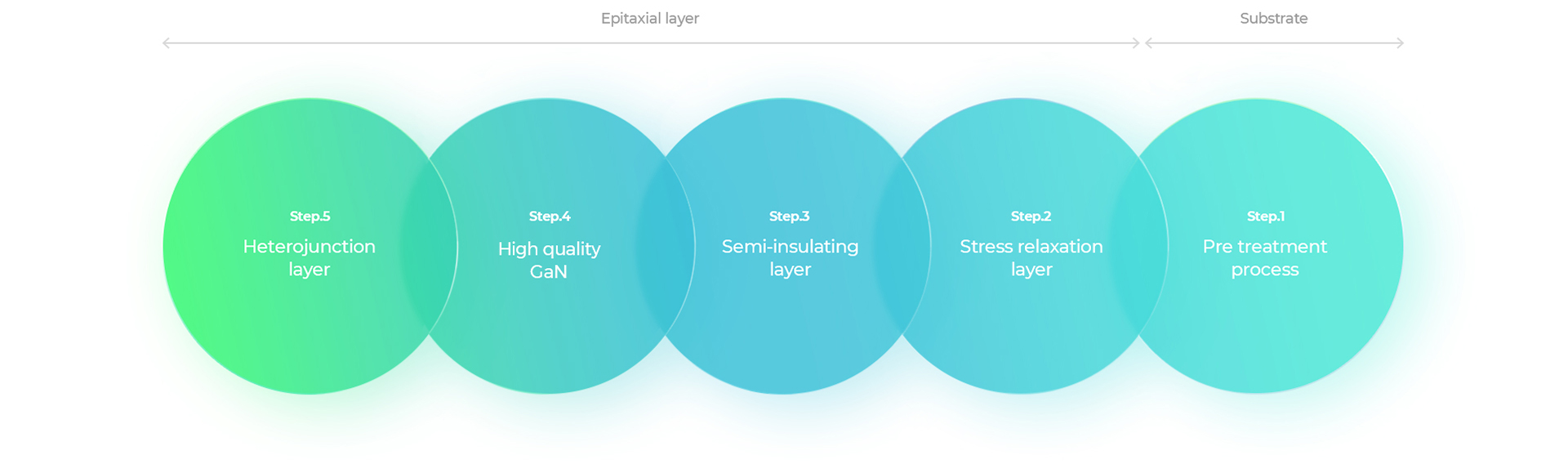
Step.1
Pre-treatment process
Remove the natural oxide film formed on the substrate surface
Step.2
Stress relaxation layer
Grow a stress relaxation layer for preventing cracks on the epitaxial layer
Step.3
Semi-insulating layer
Growth of layer that reduces the leakage current flowing toward the substrate when the electronic device is operated
Step.4
High quality GaN
Grow a layer that becomes the passage through which current flows when the electronic device operates
Step.5
Heterojunction layer
Grow a layer in which the structure of the electronic device is constructed
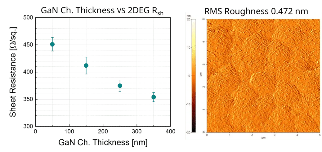
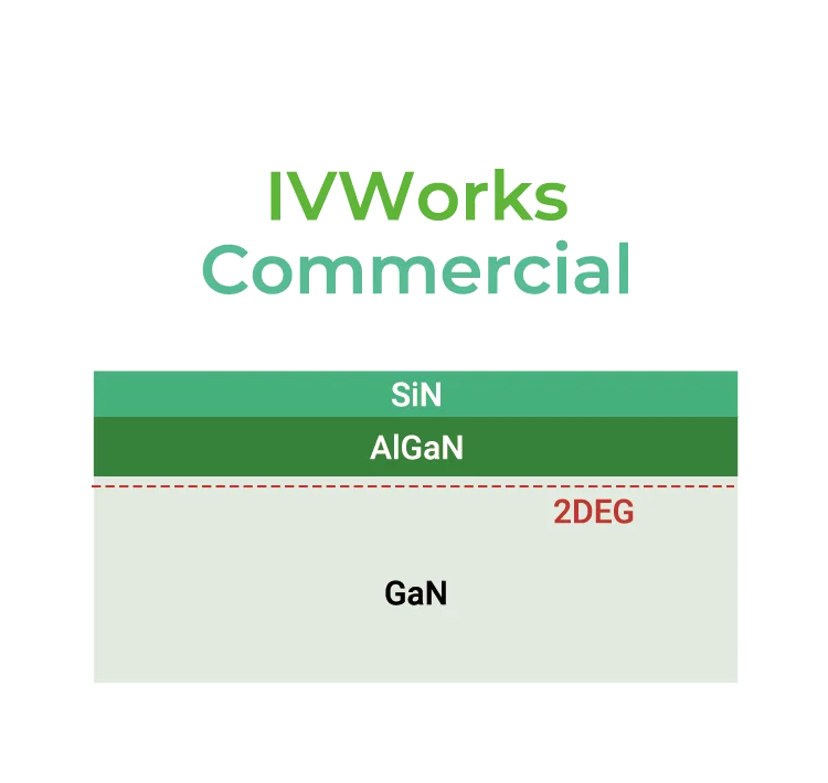
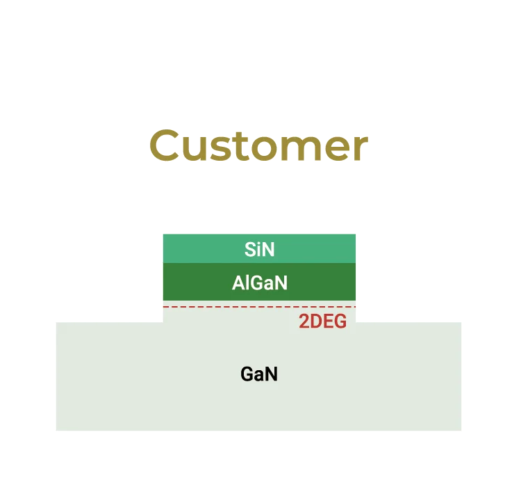
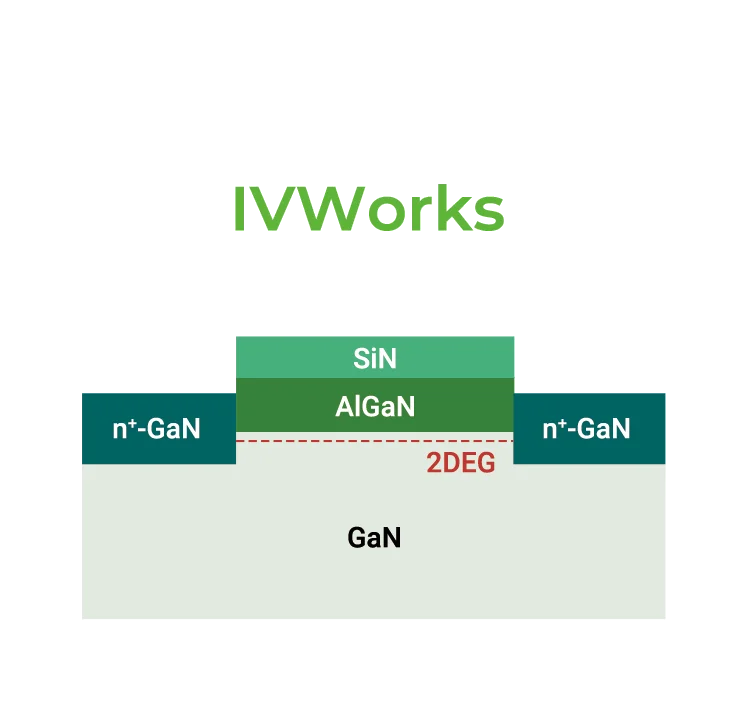
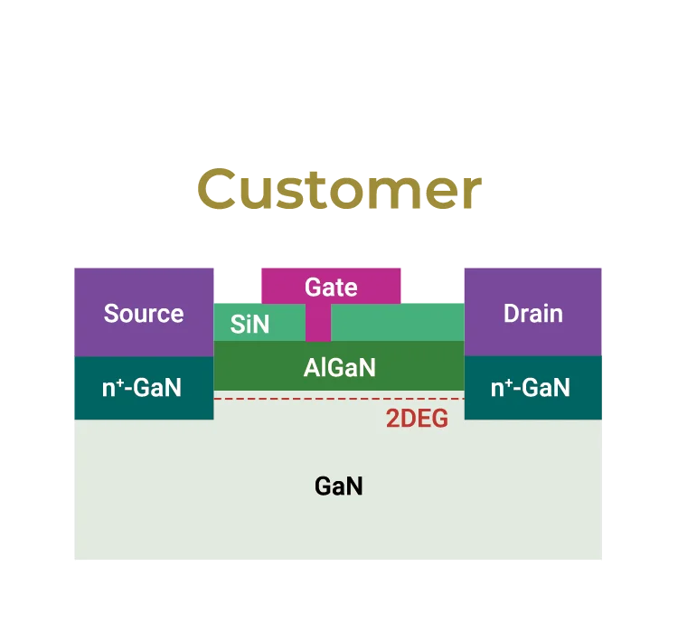
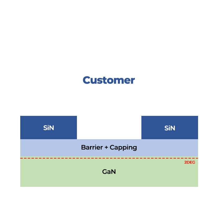
Structure and specification
| Parameter | Typical Date | Measurement |
|---|---|---|
| Barrier Thickness | 26nm±1nm | Mecury probe or TEM |
| Barrier Composition | 23%±1% | X-ray diffractometer |
| Total Thickness Uniformity | <±2% | Reflectometer |
| Wafer Bow | <±20㎛ | Stress gauge |
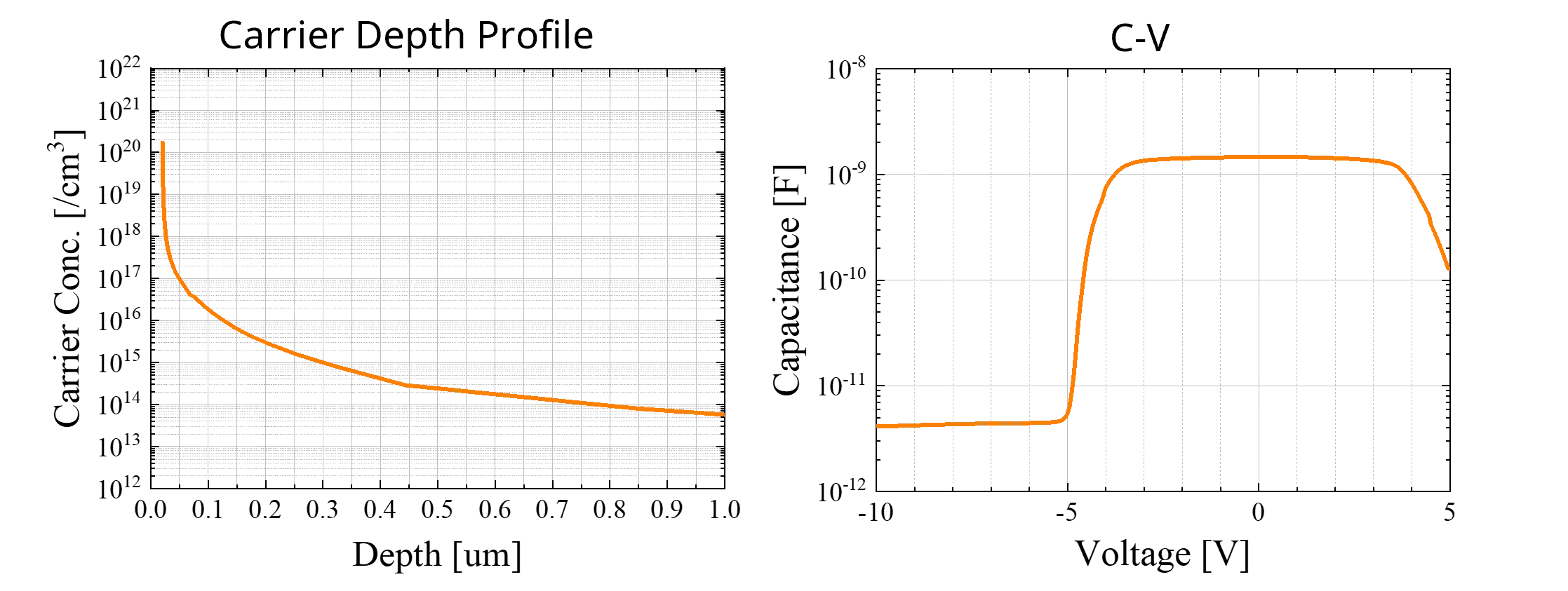
| 2DEG Mobility | 1,700~2,000㎠/Vs | Hall |
| 2DEG Density | <0.6~1.2 x. 1013/㎠ | |
| Sheet Resistivity | <<450 Ohm / sq. | Eddy current |
| Layer | Typical Date | Measurement | |
|---|---|---|---|
| Cap | GaN | 2nm | Thickness can be customized |
| Barrier | AlGaN(23%) AlN | 25nm, 1nm | Thickness and composition can be customized |
| GaN Channel | High quality GaN | 190nm | Thickness can be customized |
| Buffer | uid-AlGaN Al(Ga)N multi-layer |
1.00㎛ ,0.5㎛ ~ 1.5㎛ | Thickness and composition can be customized |
| Substrate | Silicon | 500㎛ ~ 1,000㎛ | 4inch~8inch (110),(111) High resistivity or Low resistivity |
| SiC | 500㎛ | 4inch, 6inch 4H or 6H Semi-insulating |
|
Product features
IVWorks has an advantage in the digital conversion flow for material development with its eco-friendly
automation techniques using artificial intelligence thus increasing product quality and productivity.
01
Productivity improvement
02
Product quality consistency
03
Eco-friendly material technology application
04
Streamlined manufacturing process
05
Global leading company in compound semiconductors
FAQ
-
How long does epitaxial growth take?
The development process for all products of IVWorks begins after a sufficient preliminary agreement is made in accordance with thin-film device characteristics requested by customers. Each product is customized to meet customer requirements. Therefore, the process periods may vary depending on the customer requirements.
-
How do customers purchase products?
With our proprietary Hybrid-MBE single-crystal growth technology, we offer flexible use of Al and In, along with easy doping control. This allows us to grow a wide range of epiwafer structures, including GaN, AlGaN, InGaN, AlN layers, as well as p-doped and n-doped layers.
Step 1. Submit request form – Step 2. Assign a dedicated engineer – Step 3. Product meeting (schedule and specification discussion) – Step 4. Process initiation – Step 5. Quality inspection – Step 6. Delivery of quality data and product
If you would like to purchase products or request a quote, please complete the Q&A form on our website. A assigned engineer will contact you within 1–3 business days.
-
Where can I check product prices?
All of our products are manufactured through a customized, made-to-order process tailored to each customer’s requirements, so pricing varies by product. IVWorks offers the wizdomm epidesign service, which allows customers to directly design their own epitaxial structures and receive a quotation.
The final price is determined based on the requested quantity and structure, following our internal pricing guidelines and a review by the assigned engineer.
-
How can I know if the wafers I received meet the requirements I submitted?
The crystalline property, surface resistance, electrical characteristics, etc. of grown GaN epiwafers are meticulously checked using OM, SEM, AFM, etc. before delivering epiwafers to the customers. Each customer is provided with the data collected in the process.
-
I would like to propose a technological business agreement.
Contact us via the contact information below for technological business agreements and business inquiries, and we will review them and get back to you. Inquiries on technological business agreements with IVWorks.
ivw@ivwkr.com