
news
Epiwafer Are No Longer Just for Semiconductor
In October, a seminar on the industrialization strategy of artificial photosynthesis hydrogen was held at the National Assembly of Korea. IVWorks participated as a technical session presenter, introducing its large-diameter epiwafer mass production technology. Gallium nitride epiwafers are mainly used in consumer electronics, telecommunications, and the defense industry, so one might wonder what connection they have with the hydrogen economy. But epiwafers are no longer a technology limited to semiconductors.
For Advanced Material Startups, Market Expansion Is Essential
Startups cannot survive on technology alone. When demand sources are limited and the industry scope is narrow, market fluctuations can easily lead to revenue instability. IVWorks faces the same challenge. GaN epiwafers are primarily used in power and RF semiconductor industries, with more than 90% of demand coming from overseas foundries or integrated device manufacturers (IDMs). Such dependency on specific industries and customers can make a company vulnerable to sudden external changes. Even with strong technical capabilities, startups must prepare for unpredictable risks such as semiconductor market cycles, the suspension of major customer orders, or shifts in government project priorities. Therefore, diversifying markets through the reinterpretation of core technology is essential for survival.
By supplying proprietary technology to emerging markets, companies can create new opportunities. Securing new demand opportunities not only stabilizes cash flow but also allows a company to evolve from a simple supplier to a co-developer or strategic technology partner. It also enables the establishment of a revenue model based on long-term supply agreements and gradual market expansion across different sectors.
For materials companies, growth depends on extending the applicability of their technologies into new industries. For example, the UK-based compound semiconductor company IQE has expanded beyond its traditional wireless and photonics businesses into GaN power and micro-LED applications. In a similar context, IVWorks has broadened its demand base from traditional power semiconductors to low-carbon markets, particularly in clean energy areas based on water and hydrogen. What sets IVWorks apart is its capability to uncover new demand in non-traditional industries, extending beyond the usual semiconductor-adjacent applications.
Epiwafers as the Key to Artificial Photosynthesis for Hydrogen
IVWorks has been providing contract manufacturing of epiwafers for artificial photosynthesis panels for a U.S.-based green hydrogen company for about two years. Artificial photosynthesis for hydrogen is a next-generation clean energy technology that mimics the photosynthesis process in plants to split water using sunlight and generate hydrogen.
The epiwafers used in this technology are designed with a nanowire structure, allowing efficient movement of electrons and holes under sunlight. The InGaN semiconductor layer grown on the wafer, along with a thin photocatalyst, uses the electrons to produce hydrogen (H₂) and the holes to oxidize water to generate oxygen (O₂). In other words, IVWorks’ epiwafers act as a key component in artificial photosynthesis panels, enabling the production of hydrogen from water using only sunlight.
Green Hydrogen Energy?

Hydrogen can be classified as gray, blue, or green depending on the production method. Gray hydrogen, which currently accounts for approximately 96% of global hydrogen production (2015, IEA), is produced from fossil fuels and generates about 10 kg of carbon dioxide for every 1 kg of hydrogen produced. Blue hydrogen is produced in the same way as gray hydrogen, but the resulting carbon dioxide is captured and stored. Nevertheless, because fossil fuels are still used, carbon emissions cannot be completely eliminated. In contrast, green hydrogen is produced by electrolyzing water using electricity generated from renewable energy. This process emits no carbon dioxide, making green hydrogen a highly environmentally friendly energy technology.
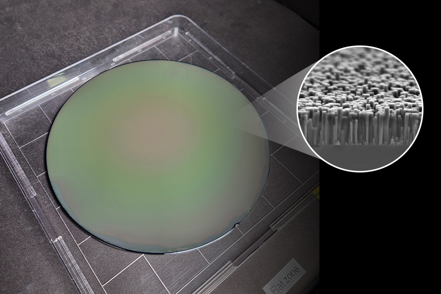
The formal name for the epiwafers used in artificial photosynthesis panels is GaN (InGaN/GaN) nanowire epiwafer. They feature a layered structure composed of InGaN and GaN. GaN serves as a robust foundation, with excellent visible-light absorption and photocatalytic properties, enabling the efficient implementation of InGaN nanowires. Nanowires are linear structures with diameters on the nanometer scale, providing a much larger surface area compared to a flat plane. By employing vertically aligned nanowire structures, light can be reflected and absorbed multiple times, promoting enhanced water-splitting reactions.
However, these structural advantages come with technical challenges. Nanowires must be grown at consistent spacing and height to ensure uniform light absorption and charge transport. Growing billions of nanowires with uniform spacing and orientation across a wafer larger than a human palm is a globally difficult technical task. Therefore, establishing a mass production system while maintaining uniform quality is not easy. Furthermore, semiconductors like GaN and InGaN have complex crystal lattices, so as the wafer size increases, it becomes even more challenging to maintain uniform thin-film growth due to variations in temperature, pressure, and gas concentration across the wafer.

Why is scaling up to large-diameter wafers necessary?
First, it allows for a larger reaction area. Artificial photosynthesis panels produce hydrogen by splitting water using sunlight, and the larger the light-receiving surface, the broader the area where the hydrogen-generating reaction can occur. Second, it enables more efficient system design. Using large-diameter wafers allows the construction of a single, larger reaction unit. For example, if a single 6-inch wafer could replace nine 2-inch wafers, the overall structure could be simplified and electrical losses reduced. Third, it improves productivity and cost efficiency. A single epitaxial growth process produces panels with a larger reaction area, reducing the manufacturing cost per unit area and increasing production efficiency. This means more hydrogen can be generated in the same amount of time or larger panels can be produced with the same equipment, which benefits the scaling up and mass production of artificial photosynthesis panels. It provides a technical foundation for advancing laboratory-level artificial photosynthesis toward industrial-scale applications, while also offering a competitive edge in the convergence of semiconductor and hydrogen technologies.
The news of IVWorks successfully scaling and commercializing 8-inch nanowire epiwafers has attracted industry attention. This is not simply a matter of increasing wafer size, but a breakthrough that overcomes the high technical barrier of uniformly growing InGaN/GaN nanowires across a large substrate.
The Era of Green Hydrogen Demands High-Efficiency Technologies
MBE Process and Two-Stage Decarbonization
As the green hydrogen market grows and the demand for advanced technologies increases, IVWorks employs a low-emission MBE process for epiwafer fabrication. In MBE, elements are thermally evaporated in a high-vacuum environment and deposited onto the substrate as molecular beams. Because the process relies on physical deposition rather than chemical reactions, direct greenhouse gas emissions, such as methane (CH4) or carbon dioxide (CO2), are minimal, and byproducts are greatly reduced. Additionally, the high-vacuum environment enables efficient material deposition, minimizing raw material waste and improving process efficiency. As a result, energy consumption and indirect carbon emissions are reduced, enabling environmentally friendly and sustainable epiwafer production. Epiwafers produced through this low-carbon process are then used in hydrogen generation, achieving a two-stage decarbonization effect that reduces carbon emissions both during production and utilization.
Materials to Solutions : Technology Unlocking New Industries
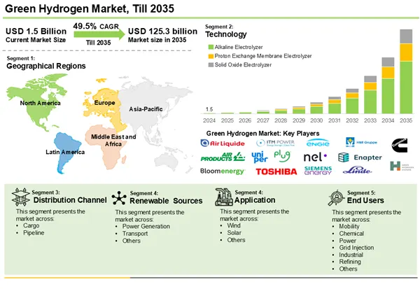
The global energy market is rapidly transitioning from a power-centric system to an integrated framework combining electricity, heat, and hydrogen. The green hydrogen market is projected to grow at an annual rate of 49.5%, reaching approximately USD 125.3 billion by 2035. This rapid expansion highlights the critical role of advanced material technologies in maximizing hydrogen production efficiency. In response, IVWorks has advanced the scaling and mass production stabilization of GaN nanowire epiwafers for artificial photosynthesis-based hydrogen generation. This achievement enables high-efficiency, low-carbon processes and establishes a new growth axis by extending semiconductor-based precision growth technologies into the energy sector.
IVWorks is evolving beyond being a mere semiconductor material supplier into a solutions provider that bridges technology and market needs. The wafers themselves act not just as materials but as connectors for technological application, creating value in new industrial domains. Through the scaling and commercialization of nanowire epiwafers, we have established tangible intersections with the emerging energy industry. Moving forward, such technological expansion will continue to break down industrial boundaries and lay the foundation for a new solutions market linking semiconductors to energy.
Yoon-Seo Cho l Marketing Manager at IVWorks
Ji-Min Park l Strategy Planning Senior Staff at IVWorks
※This article reflects the subjective opinions of the contributor and may differ from the official position of IVWorks
news
How AI-Agents Are Transforming the Materials Ecosystem, Part 2: From Lab to Mass Production
Editor’s Note:
This post is the second part of the three‑part series titled “How AI‑Agents Are Transforming the Materials Ecosystem.” In the previous article, we introduced the basic concept of AI‑Agents and discussed why semiconductor materials companies are looking to build them. In this second installment, we focus on epitaxial wafer production examining AI‑Agents from a manufacturing perspective and how they are being applied. As before, this series emphasizes insights over technical detail, serving as a primer to help you better understand future technical columns. Please feel free to comment with any questions. We appreciate your interest in IVWorks’ AI research!
Traditional Epitaxy Methods and Their Limitations
Epitaxial growth, a process considered the most critical step in securing a stable supply of gallium nitride semiconductors, involves layering extremely thin films on a substrate at the atomic level. This is an extremely delicate and complex procedure, as it requires nanometer-level precision in controlling physical reactions that occur under high-temperature and high-vacuum conditions. Despite its sophistication, the traditional methods of epitaxial growth that have been used until now reveal several limitations. These are not necessarily technical flaws, but rather commercial constraints that become evident in mass production environments.
A Slow Cycle for Quality Improvement
◇ Immediate decisions and interventions to prevent process risks
Epitaxy is inherently unsuitable for parallel experimentation. Typically, it follows a cycle of ‘growth → condition adjustment → regrowth’. If the measurement results of the grown wafer fall short of the target, parameters such as flux, temperature, doping concentration, and growth rate are adjusted, and the growth process is repeated. This cycle is repeated multiple times until the desired epitaxial structure is achieved—a method that has long been used in both research and industrial settings.
At first glance, waiting for potentially defective wafers to finish growing might seem inefficient. Depending on the method used (MBE, MOCVD, HVPE, etc.), epitaxy is typically conducted in sealed environments. Since it’s difficult to visually inspect progress during the process and not feasible to test multiple conditions simultaneously due to equipment constraints, the only viable strategy is to finely tune and verify each condition through repeated trials.
However, this also means that improvement cycles are slow, and process optimization often depends heavily on the engineer’s experience and intuition. While some tools like RHEED, reflectometry, or pyrometers, do allow partial real-time monitoring, interpreting these signals still requires human judgment. Whether a signal variation indicates an anomaly or falls within acceptable bounds is ultimately a subjective call. As a result, different engineers may interpret the same data differently, and crucial signals can sometimes be overlooked. This makes real-time error detection during growth difficult, and in most cases, issues with process conditions are only recognized after the run is complete.
◇ High Experimental Costs Due to Repeated Cycles
Because parallel experimentation is structurally difficult and continuous human oversight is required, each experimental run demands significant time and resources. When accounting for setup, parameter adjustment, processing, post-treatment, and analysis, even a single cycle can take several hours or even dozens of hours. As the number of iterations increases, the cumulative cost in both time and money becomes substantial. In real-world production settings, it is not feasible to repeat such experiments indefinitely. This ultimately places constraints on manufacturing throughput.
Challenges in Reproducibility and Consistency
◇ A Process Without a Clear “Correct” Answer
Another key challenge of epitaxial growth lies in its numerous variables, which are often nonlinearly interrelated. This makes it nearly impossible to pre-calculate the exact optimal conditions. Typically, parameters are set based on expert experience and historical data. However, even with identical settings, outcomes may vary due to changes in equipment condition or environmental factors. In such uncertain and complex scenarios, it’s difficult to reliably identify optimal conditions using traditional experimental methods alone. In mass production, reproducibility and consistency of process conditions are critical. While it may be possible to achieve a certain quality level in small-scale experiments, replicating the same results reliably in a full-scale production environment is a far more challenging task.

Why Should We Address These Limitations?
The compound semiconductor industry has not yet reached maturity. Unlike silicon-based semiconductors, compound semiconductors such as GaN and InP have a relatively short commercial history, and both the technology and its ecosystem are evolving rapidly. This means that companies able to establish a technological edge early on are far more likely to dominate the market in the long term.
However, quality alone is not enough.
A certain level of quality is now considered a basic, non-negotiable requirement in the market. Customers increasingly prefer partners who can not only maintain high quality but also offer shorter lead times and greater flexibility in delivering custom specifications. Due to the complex composition and intricate processing of compound semiconductors, there is significant pressure to achieve maximum results from each experiment and production run. As market trends sift rapidly and development speed itself is now seen as a key competitive edge, failing to eliminate inefficiencies in this changing environment will inevitably lead to falling behind in the competition.
The problem is that traditional production methods alone are no longer sufficient to meet these demands.
In manufacturing, cost and time are crucial. As we’ve seen earlier, the traditional approach of optimizing process conditions one by one through experimentation is costly and time consuming, making it difficult to respond quickly maintain consistent quality. Moreover, relying solely on engineers’ experience to predict and reproduce the complex interactions among dozens of variables is increasingly unrealistic. These limitations stand in direct conflict with evolving market expectations.
This is why IVWorks is striving to gain a technological edge through the automation and intelligent transformation of epitaxial growth processes. The goal goes beyond simply replacing human labor with AI. What’s needed is a system that can reliably analyze processes based on data, predict potential failures in advance, learn the complex interdependencies among variables, and propose or adjust optimal epitaxy conditions autonomously. The AI-based epitaxial process innovation led by IVWorks has now attracted the attention of latecomer companies. But IVWorks’ automation efforts are not merely aimed at operational efficiency—they serve as critical technological infrastructure for solidifying a leadership position in the GaN market, where neither industry standards nor market dominance have yet been clearly established.
Reflecting on the limitations discussed above, several natural questions arise:
‘Is there a way to accelerate the improvement cycle?‘
‘Can we grow high-quality epitaxial layers from the start, without needing to adjust conditions later?‘
‘Is it possible to dramatically improve productivity?‘
‘What if engineers didn’t need to be constantly monitoring equipment? What if human error could be minimized? What if optimal growth conditions could be pre-calculated?‘
If ideas like these can be realized, it would open a path toward overcoming the fundamental structural constraints of epitaxial processing.
Case Study: Optimizing Epitaxy Productivity with AI Agents
In a previous article, we introduced IVWorks’ AI Agent as a concept that integrates and expands various automation elements required for epitaxial growth. Today, we’ll take a closer look at one of its core components: MRA (MBE Run Automation). Planned by a task force composed of AI engineers and epitaxy specialists last year, MRA has recently begun implementation on real production lines. This project literally means “run automation,” that is, an unmanned autonomous production system where AI independently operates the MBE epitaxial growth process.
The key concept is “human absence.”
Epitaxial growth continues without requiring an engineer to be physically present. Let’s explore what that actually means.
Human Intervention in Epitaxy: Still Essential
◇ Real-Time Decisions and Intervention to Mitigate Process Risks
To produce high-quality epitaxial wafers, various parameters across multiple stages, from wafer loading and vacuum creation to run readiness, growth, and cooling must be managed and adjusted in a timely manner. In the past, operators had to manually press “Start” at each step. Today, built-in software automates the sequence, allowing the process to progress on its own. However, this automation follows only a predefined mechanical flow and cannot respond to real-time issues such as physical anomalies or system errors.
When unexpected changes occur, such as vacuum fluctuations, equipment malfunctions, or temperature variations, real-time judgment and response are needed. In such cases, human intervention becomes necessary. That’s why, traditionally, engineers have always had to be present during the epitaxial process.
Let’s take the “wafer loading issue” as an example.
The first step in epitaxy is to place the wafer holder into the loading chamber. In an MBE system, multiple chambers are connected, and a robotic arm transports the holder between them. But what happens if the holder is slightly misaligned? It may collide with internal components during transfer or cause the wafer to tilt and crack.
Loading errors can occur for a variety of reasons.
These include wafer contamination, holder wear, coordinate misalignment, and systemic factors like temperature gradients or vibrations inside the equipment. Errors can also stem from initial setup issues or physical misalignments. Such loading problems can lead to compositional imbalances, crystal defects, or complete growth failures, making it difficult to produce high-quality wafers.
What’s more, these issues can cause significant system-level losses. For example, if a holder is dropped inside the chamber, the vacuum that has been built up over several hours must be broken to recover it. This triggers a time-consuming recovery process, often requiring source re-deposition and delaying the entire production schedule by more than a week. Beyond material costs, the indirect losses from disrupted production are substantial. To avoid such risks, engineers have traditionally monitored equipment continuously during each run, responding immediately to any signs of abnormality.
And this issue is not limited to the loading stage alone.
During thin-film growth, real-time responses to a wide range of variables are also essential. These include maintaining and adjusting growth conditions, detecting crystal states via RHEED patterns, determining whether to halt the process when vacuum gauge warnings occur, and stabilizing cell temperatures. Because such decisions require quick and accurate responses, engineers have historically been unable to leave the production line unattended during epitaxial growth.
◇ What changes with MRA?
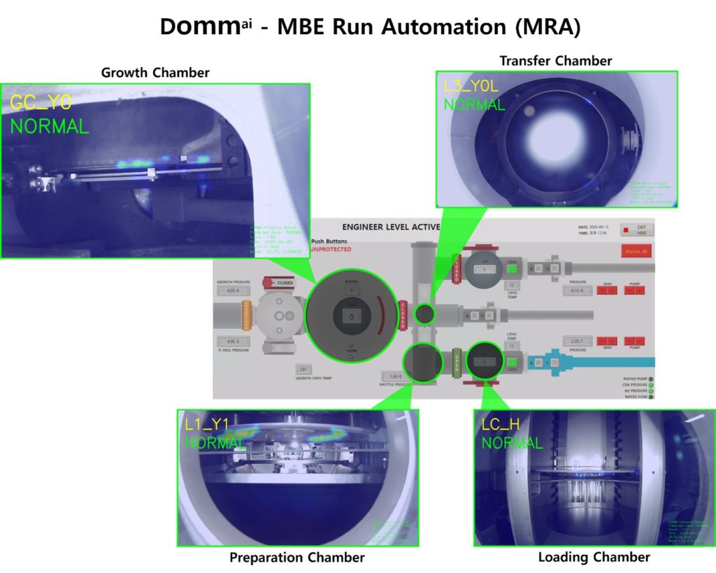
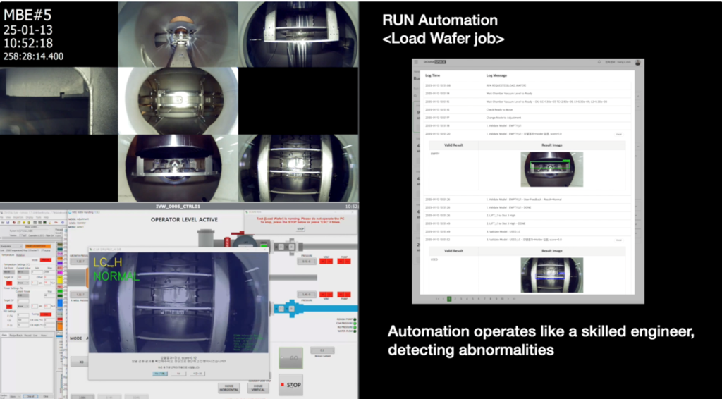
The image below shows a wafer holder being loaded into the chamber. MRA continuously analyzes the movements of both the wafer and holder in real time and calculates an anomaly prediction score, a numerical representation of how much the current state deviates from the normal. The AI model learns from historical process data and equipment behavior patterns, then compares them against real-time movement. If current behavior strays outside the expected range, MRA instantly detects the abnormality (as seen in the “abnormal” state on the right).

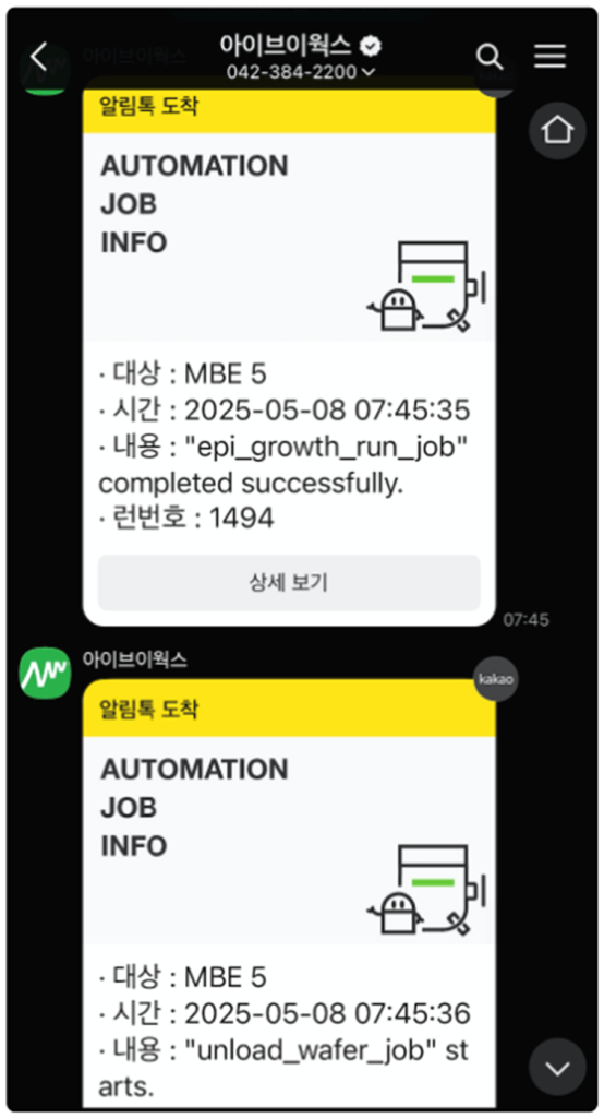
In such cases, MRA can autonomously halt the task based on its own judgment. Depending on the situation, it may also prompt the operator with a set of options and request a new task. Every event and action that occurs during the process is communicated to the engineer in the form of a message. These messages include real-time process footage along with explanations of the detected risks and the system’s corresponding responses. This means engineers no longer have to physically stand next to the machine to oversee the process. They can remotely monitor the wafer loading stage and remain fully informed about the status of the run without missing any critical information.

MRA operates reliably even during nights and weekends when no operators are on site. Individual process steps, including wafer loading, can be scheduled for automatic execution. Operators can predefine the sequence and timing of tasks in advance, allowing processes to run unattended outside of regular working hours. This resolves a major limitation of traditional methods, where processes were constrained by operator availability. Now, production can continue reliably even during off-hours, contributing significantly to improved productivity. This system is already in full operation at IVWorks’ fabrication facility.
For foundries, where mass production and sales are the ultimate goals, productivity is a critical factor. Companies must complete as many meaningful runs as possible within limited working hours. In this context, MRA not only ensures consistent quality but also enables the production of more high-quality wafers within the same time frame.
Although we’ve focused on a single use case here, MRA functions as if a highly experienced engineer were monitoring the production line 24/7. It detects abnormalities at every stage in real time, makes appropriate judgments based on the situation, and can even notify the operator or present response options when necessary. This represents more than just automation—it’s a shift toward autonomous processing, where the system can perceive, decide, and act on its own.
Today, we’ve explored the limitations of traditional epitaxial methods and introduced a small-scale application of MRA as a solution for improving production in mass manufacturing environments. In the next installment of this series, we’ll take a closer look at how IVWorks is concretely addressing the ideas and challenges that emerged from those limitations.
Yoon-Seo Cho l Marketing Manager t at IVWorks
※This article reflects the subjective opinions of the contributor and may differ from the official position of IVWorks
news
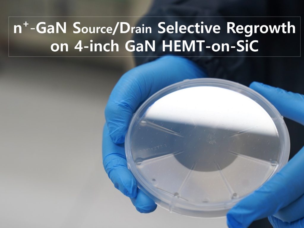
IVWorks’ n⁺-GaN regrowth service is the optimal choice for customers aiming to realize high-performance GaN HEMTs. It is not only ideal for university research teams pursuing top-level academic results, but also for GaN foundries and IDMs seeking to deliver differentiated device performance to the market. With minimal resource input, IVWorks enables customers to achieve maximum process effectiveness.
This n⁺-GaN regrowth process order was received from an Asian university.
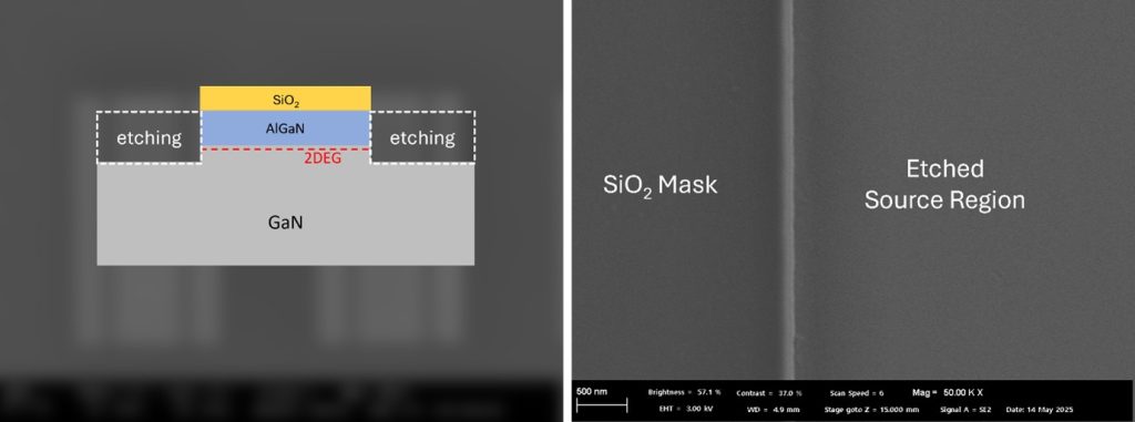
IVWorks performs selective area growth of n⁺-GaN only in the source and drain regions at a low temperature of approximately 700 ℃. This approach can reduce contact resistance(Rc) by nearly one tenth, while enabling non-annealed ohmic contact without the need for RTA of ohmic metals. As a result, it effectively eliminates various degradation issues typically caused by the RTA process.
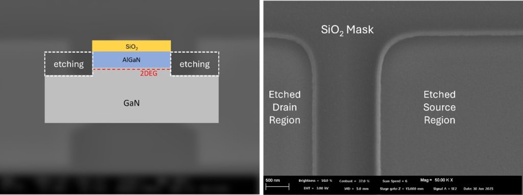
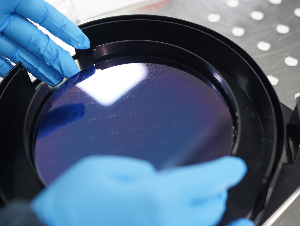
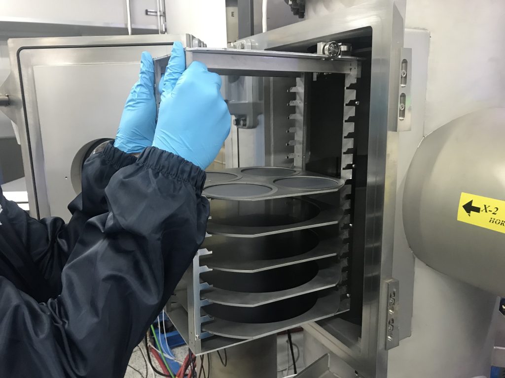
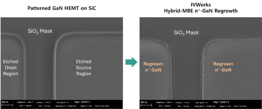
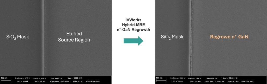
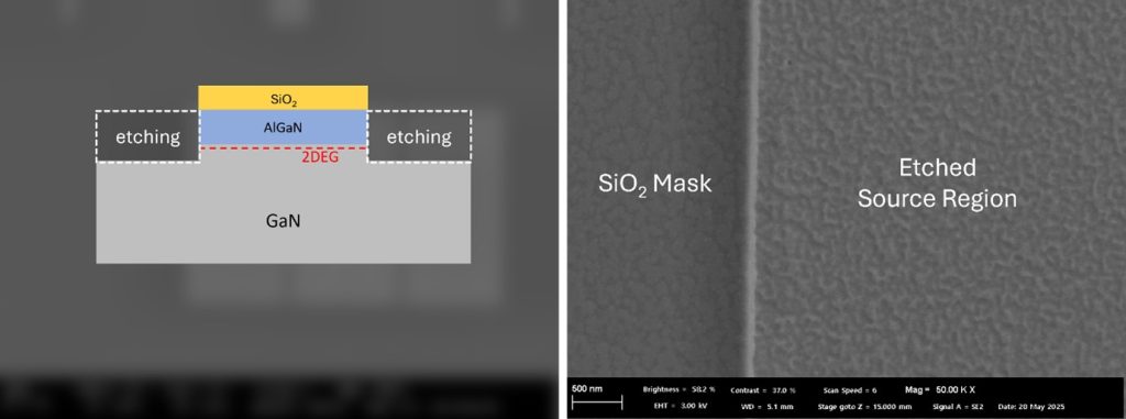
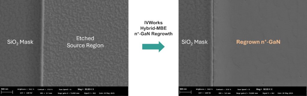
At IVWorks, when we receive patterned wafers from a customer, the first step is to inspect the etched surface of the source and drain regions where selective regrowth is to be performed, using SEM measurements.
The patterned wafer we received for this process was masked using SiO₂. Both SiO₂ and SiN are ideal mask materials for IVWorks’ selective area regrowth, ensuring that no growth occurs in the masked regions. As a result, n⁺-GaN is grown exclusively in the source and drain areas, with complete selectivity maintained after regrowth. The patterned wafer provided by this customer had a very clean etched surface in the source and drain regions, which is expected to allow smooth regrowth.
Although we occasionally receive wafers with rough etched surfaces, IVWorks has established both ex-situ and in-situ cleaning procedures, along with initial growth conditions optimized for surface recovery during the early stage of regrowth. Thanks to these capabilities, surface recovery is generally achievable, and the desired n⁺-GaN properties in the source and drain regions can be reliably obtained.
(*For reference on regrowth over rough etching – 4″ GaN HEMT with n⁺-GaN S/D Selective Regrowth for Asian University)
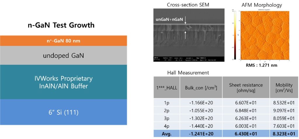
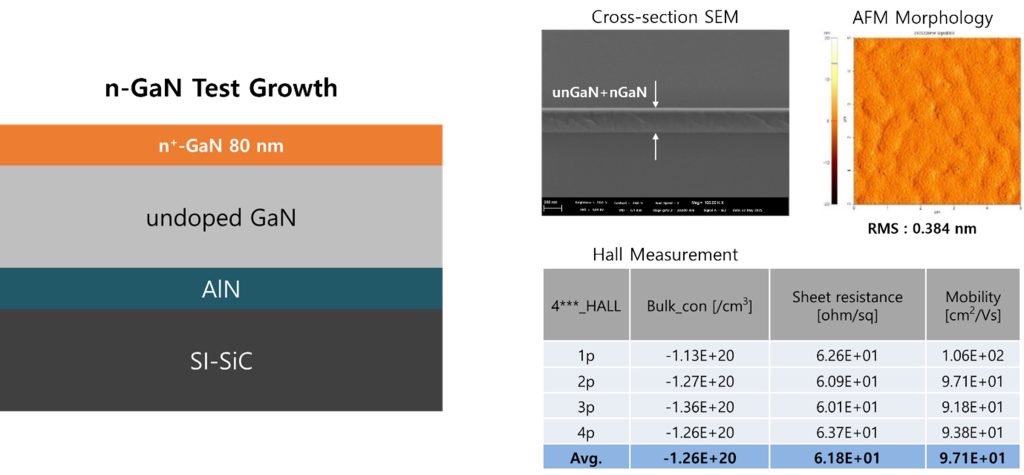
At IVWorks, before performing n⁺-GaN regrowth on customer wafers, we first grow an n-GaN test wafer using the same material and wafer size as the customer’s, under the exact same growth conditions intended for the regrowth. This allows us to verify the n-type doping characteristics in advance, ensuring a high level of process accuracy. For this particular process, we also developed and applied a modified growth condition at the customer’s request, in order to further increase the n⁺-GaN doping concentration.
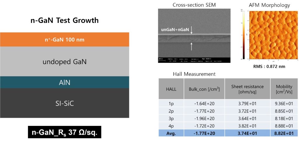
Using a 4-inch SI-SiC wafer identical to the patterned wafer provided by the customer, we applied the newly developed growth condition to perform n-GaN test growth. The results confirmed both the precise growth rate and n-type doping characteristics. A high doping concentration of 1.77×1020 cm⁻³ was achieved, and the sheet resistance was measured at 37ohms/sq, which is approximately half the value obtained under the previous growth condition. Based on these results, we are now proceeding with the growth on the customer’s patterned wafer using this updated condition.
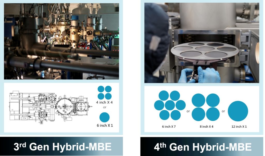
IVWorks grows n⁺-GaN using its proprietary Hybrid-MBE system. Now in its fourth generation, the Hybrid-MBE platform supports n⁺GaN regrowth on wafer sizes ranging from 2 inches to 12 inches. In addition, IVWorks has established a fully autonomous production system by integrating the entire epitaxial wafer production workflow into its proprietary AI agent framework called Domm.
Using IVWorks’ Hybrid-MBE and regrowth technology, n⁺-GaN regrowth was successfully completed on the patterned wafer provided by the customer. Perfect selective area growth was achieved, with no growth observed in the masked regions, and n⁺-GaN was grown only in the source and drain regions. The regrown n⁺-GaN layer reached a thickness of 100㎚, maintained 2D-mode growth, and formed proper epitaxial contact with the 2DEG sidewalls.

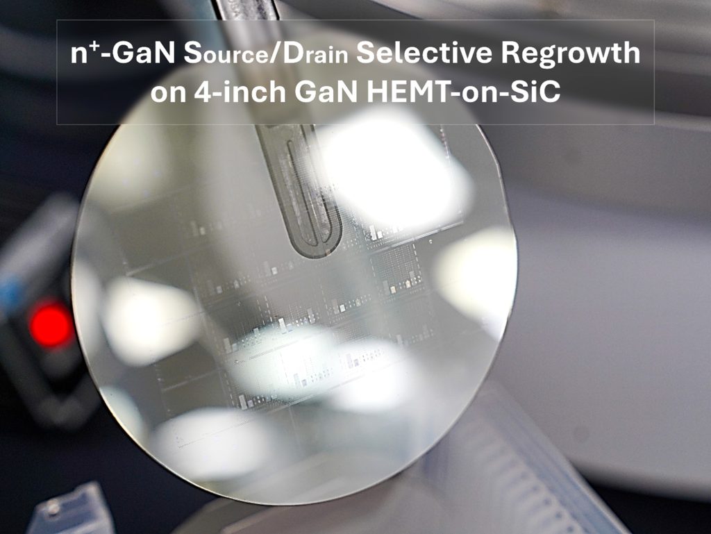
The wafer with n⁺-GaN selectively regrown in the source and drain regions of a 4-inch GaN HEMT on SiC has been vacuum sealed and successfully shipped to the customer.
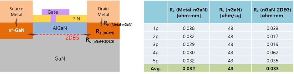
Using the newly developed n⁺-GaN regrowth condition, we observed excellent contact resistance results.
The measured contact resistance between the ohmic metal and n⁺-GaN (Metal to nGaN) was 0.032ohm·mm, and the contact resistance between the n⁺-GaN and 2DEG(nGaN to 2DEG) was 0.033ohm·mm. We received very positive feedback from the customer, who was highly satisfied with these results.
Inquiries │IVWorks Website QNA or www.domm.ai/contact
news
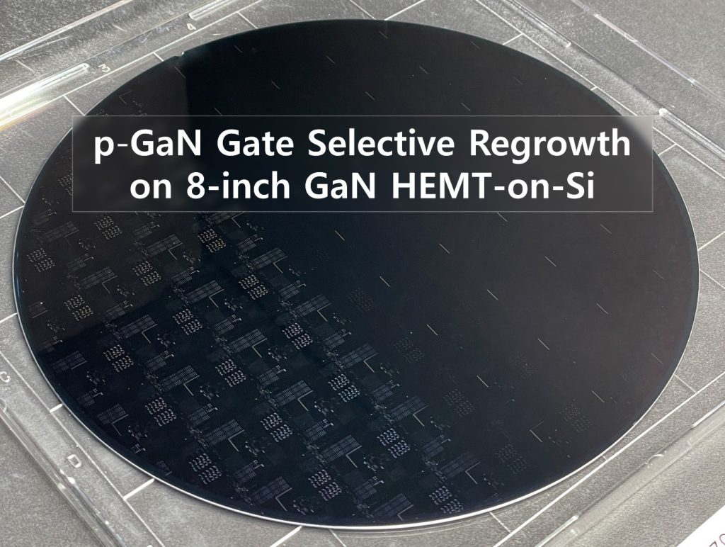
Selective p-GaN Regrowth on 3D FIN Structure of 8″ RF GaN HEMT on Si for a U.S. Customer
We’ve recently received a process order for p-GaN regrowth from a U.S.-based company.
IVWorks specializes in selective area growth services using our proprietary large-scale Hybrid-MBE system, autonomously operated by AI. In addition to GaN HEMT and microLED epiwafers, we support a wide variety of custom regrowth structures. You can design your own epitaxial structures—including p-GaN regrowth and n⁺-GaN regrowth—and get instant quotes directly here.
Just like this project, our ‘p-GaN regrowth’ service enables selective area growth in the Gate region at low temperatures around 700°C—a highly effective solution for implementing normally-off GaN HEMTs. In the rapidly growing communications market, RF-GaN HEMT on Si technology is gaining strong attention—especially for mobile device applications, where minimizing standby power consumption and enabling low-power operation is essential. To achieve this, normally-off RF-GaN HEMT technology is required.
There are two main approaches to implementing normally-off behavior in RF-GaN HEMTs: One is the gate recess method, which thins the barrier layer under the gate through precise etching to suppress 2DEG formation. The other is the p-GaN gate approach, where a p-GaN layer is placed under the gate to deplete the 2DEG channel. The gate recess method, especially when combined with gate length scaling, offers excellent RF performance. However, it comes with challenges in process complexity, threshold voltage stability, uniformity, and typically exhibits higher gate leakage currents.
On the other hand, the p-GaN gate method increases the vertical distance between the gate and the 2DEG due to the thickness of the p-GaN layer, and etching damage can limit aggressive gate scaling—resulting in slightly reduced RF performance. However, this approach allows for simplified processing: the p-GaN layer is grown during epitaxy and patterned to leave the gate region only. With precise control over p-type doping levels and layer thickness during growth, it enables excellent control of threshold voltage characteristics and gate leakage. In summary, the gate recess approach is preferred when maximizing RF performance is the top priority, while the p-GaN gate method is better suited for applications requiring stable normally-off behavior and process simplicity.
IVWorks’ p-GaN regrowth service offers a distinct advantage: since p-GaN is selectively regrown only in the gate region, it eliminates the need for etching the p-GaN layer—avoiding etch-induced damage and enabling the formation of narrow p-GaN gates with improved RF characteristics. In addition, because the regrowth is performed in an ultra-high vacuum MBE chamber, hydrogen compensation in Mg-doped GaN is significantly suppressed. As a result, high hole concentrations can be achieved even with relatively low Mg doping levels, and no additional activation process is required.
The precise growth control offered by MBE also makes it possible to perform regrowth on 3D gate structures, providing further design flexibility.
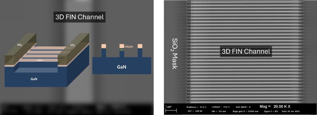
For this project, the customer provided an 8-inch GaN HEMT on Si patterned wafer, with the goal of implementing a final device structure featuring a 3D FIN gate. Accordingly, the selective p-GaN regrowth area was fabricated as a 3D FIN channel structure. The patterned wafer with 3D FIN channels was patterned with SiO₂ as the mask material. Both SiO₂ and SiN are optimal for IVWorks’ selective area regrowth process—no growth occurs on the masked regions, and p-GaN is grown only in the mask-open areas. In this project, the 3D FIN channels were formed as narrow multi-channel structures, with very tight spacing between channels.
Based on our experience at IVWorks, selective area growth is reliably achievable down to ~100㎚, and with sufficiently clean and precise mask etching, we believe growth is possible even at dimensions as small as tens of nanometers—or even just a few nanometers. At IVWorks, before performing p-GaN regrowth on customer wafers, we first grow a p-GaN test wafer using the same substrate material and wafer diameter.
This test is conducted under the exact same growth conditions intended for the final regrowth, allowing us to verify p-type doping conditions in advance—ensuring high process accuracy and reliability for the customer’s wafers.
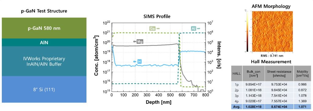
For this project, we grew a p-GaN test structure on an 8-inch Si(111) wafer, identical to the patterned wafers provided by the customer. The p-GaN layer was grown to a thickness of 58㎚ to enable Hall measurements, with an insulating buffer structure grown beneath it on the Si wafer. Growing GaN on a Si substrate is significantly more challenging than on other wafers such as SiC, Sapphire, or free-standing GaN. It requires overcoming lattice mismatch and crystal structure differences between Si and III-nitride films, while precisely managing thermal expansion mismatch, film stress, and maintaining high insulating properties in the buffer layer. Moreover, since direct contact between gallium and the silicon wafer can cause melt-back etching, the system must be carefully operated to prevent any gallium exposure to the Si surface during growth.
To address these challenges, IVWorks applies its patented InAlN/AlN superlattice buffer technology in its GaN-on-Si epitaxy platform. This buffer structure maintains high superlattice bandgap energy for strong insulation, while using the lattice mismatch between InAlN and AlN to precisely control film stress. This platform is highly versatile and can be applied to both RF GaN HEMT on Si and DC power GaN HEMT on Si epitaxial structures.
The growth of the p-GaN test structure confirmed both the accurate growth rate and the desired p-type doping characteristics. SIMS analysis showed a sufficient Mg doping concentration of ~5 × 1019 cm⁻³, and as mentioned earlier, the Hybrid-MBE environment resulted in extremely low hydrogen incorporation. Hall measurements confirmed a hole concentration of 1.0 × 1018 cm⁻³, verifying that the doping levels met the customer’s requirements. Based on this, we proceeded with a 50㎚ p-GaN regrowth on the customer’s patterned wafers under the same growth conditions.
IVWorks grows p-GaN using its proprietary Hybrid-MBE platform, now in its 4th generation, supporting epitaxy services for wafer diameters ranging from 2-inch to 12-inch. Furthermore, IVWorks has established a fully autonomous epitaxy production system by integrating all production processes with Domm, our proprietary AI agent framework.
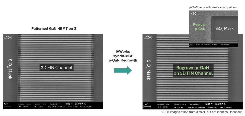
p-GaN regrowth was successfully completed on both the p-GaN gate regions and the selective area growth test patterns of the customer’s patterned wafer. Selective area growth was perfectly realized—no growth occurred on the masked regions, and p-GaN was grown only where intended. The regrown 5㎚ p-GaN layer in the 3D FIN channel regions followed the 3D geometry precisely, forming epitaxial contact on both the sidewalls and top surfaces of the FIN structures.
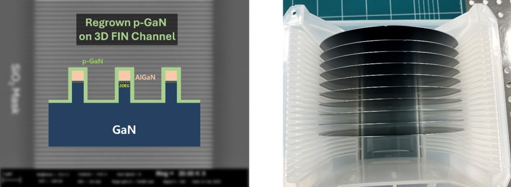
The wafer, with p-GaN selectively regrown in the 3D FIN channel regions of an 8-inch RF GaN HEMT on Si, has been vacuum-packed and successfully shipped to the customer. IVWorks’ p-GaN regrowth service supports wafer sizes from 2 inches to 12 inches, and is compatible with GaN HEMT structures on Si, SiC, GaN, and Sapphire.
Inquiries │IVWorks Website QNA or www.domm.ai/contact
news
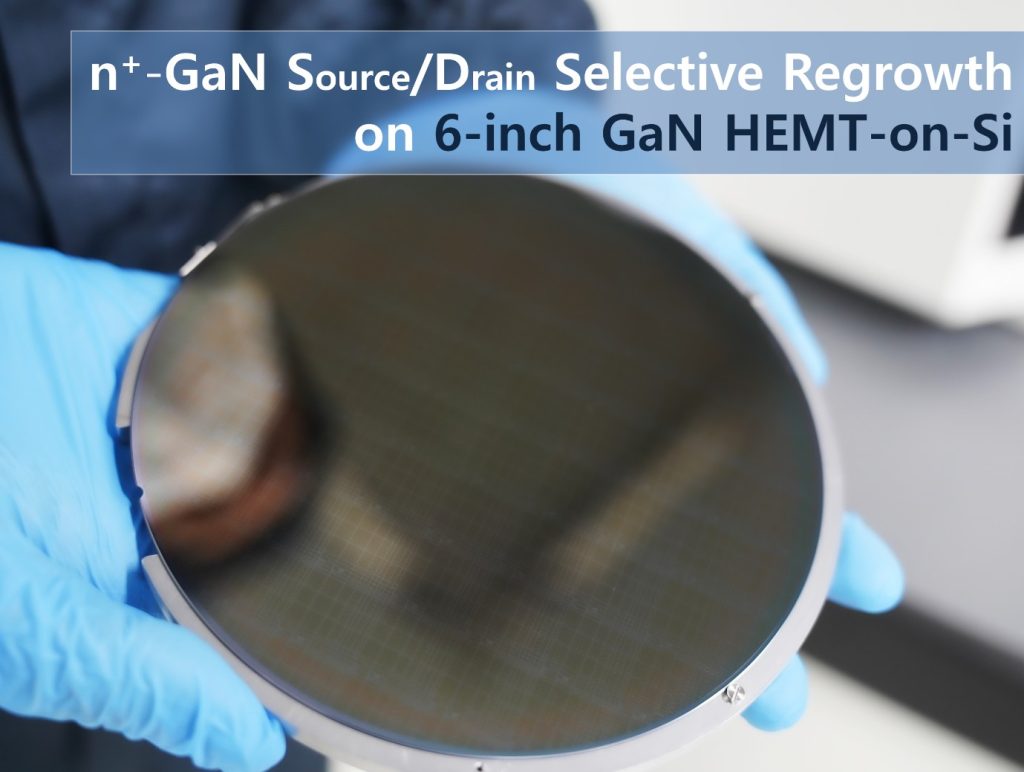
We have received a process order for n⁺-GaN regrowth from a company in the Asia region.
The patterned wafer provided by the customer is a 6-inch GaN HEMT on Si. RF GaN HEMT on Si technology is attracting strong market interest in relation to next-generation mobile communication applications. In particular, for mobile device applications, cost competitiveness is a fundamental requirement. Therefore, securing economic viability through a large-diameter wafer roadmap—from 6-inch to 8-inch to 12-inch—is essential, and GaN HEMT on Si plays a key role in enabling that transition.
Moreover, as the frequency bands of next-generation mobile communication are expected to integrate both the FR3 band (7–24 GHz) and satellite communication band (1–2 GHz), it becomes even more important to enhance performance and efficiency using GaN HEMT on Si technology. IVWorks’ n⁺-GaN regrowth process service supports not only 6-inch GaN HEMT on Si, but also 8-inch and 12-inch wafers. In addition, n⁺-GaN regrowth is available for various substrates including GaN on SiC, GaN on GaN, and GaN on Sapphire.
At IVWorks, n⁺-GaN is selectively grown only in the source/drain regions at a relatively low temperature of around 700°C. This enables non-annealed ohmic contact without the need for ohmic metal RTA, and allows contact resistivity to be easily reduced below 0.1 Ω·mm. This is a specialized epitaxy service unique to IVWorks. You can now design a wide range of epitaxial structures—including n⁺-GaN regrowth and p-GaN regrowth—and get instant quotes in real time at domm.ai/epidesign.
At IVWorks, when we receive patterned wafers from customers, the first step is to inspect the etched surfaces of the Source/Drain regions—where selective regrowth will take place—using SEM measurements.
The patterned wafers we received for this order used SiO₂ as the mask material. Both SiO₂ and SiN are ideal mask materials for IVWorks’ selective area regrowth process—no growth occurs on the masked regions, and n⁺-GaN is grown exclusively in the Source/Drain areas.
The patterned wafer provided by this customer, as expected from a high-volume production company, had a very clean etched surface in the source/drain regions. As mentioned in our previous post, etching processes vary by customer, so the surface conditions after etching can differ case by case. In particular, compared to production companies, etched surfaces from research institutes or university labs tend to be rougher and less uniform. To address this, IVWorks applies initial growth conditions that maximize surface recovery at the beginning of the regrowth process, minimizing the impact of etching surface variation. Based on our experience, as long as there is no residual mask material (such as SiO₂ or SiN) left on the etched surface, recovery is usually achievable.
So don’t hesitate to try n⁺-GaN regrowth, even if your etching process is not yet fully optimized.
At IVWorks, before performing n⁺-GaN regrowth on customer wafers, we first grow an n-GaN test wafer under the exact same growth conditions intended for the regrowth process. This test is conducted on a wafer that matches the customer’s in material and wafer size, allowing us to verify the n-type doping conditions in advance. By doing so, we ensure high process accuracy and consistency for the final regrowth on the customer wafer.
For this project, we grew an n-GaN test structure on a 6-inch Si(111) wafer, identical to the patterned wafer provided by the customer.
Growing GaN on Si wafers is significantly more challenging than on other substrates such as SiC, Sapphire, or free-standing GaN. It requires overcoming lattice mismatch and crystal structure differences between the Si substrate and the III-nitride films, while precisely managing thermal expansion mismatch, film stress, and maintaining insulating properties of the buffer layers. Additionally, since direct contact between gallium and the silicon wafer can lead to melt-back etching, special care must be taken to prevent gallium exposure to the Si surface during growth.
IVWorks provides a GaN on Si epitaxy platform using its proprietary patented InAlN/AlN superlattice buffer technology. The InAlN/AlN superlattice buffer maintains a high superlattice bandgap energy to enhance insulating properties, while leveraging the lattice mismatch between InAlN and AlN to precisely control film stress.
This technology can be flexibly applied to both RF GaN HEMT on Si and DC power GaN HEMT on Si epiwafer structures.
Following the growth of the n-GaN test structure, we confirmed the exact growth rate and n-type doping characteristics. With an n-doping concentration of 1.24e20 cm⁻³, sufficient doping was verified, and growth on the customer’s patterned wafer will proceed under the same conditions.
IVWorks grows n⁺-GaN using its proprietary Hybrid-MBE system, developed in-house.
Currently in its 4th generation, the Hybrid-MBE platform supports n⁺-GaN regrowth on wafers ranging from 2-inch, 4-inch, 6-inch, and 8-inch up to 12-inch in diameter. For an introduction to Hybrid-MBE, please refer to: 4″ GaN HEMT with n⁺-GaN S/D Selective Regrowth for Asian University
IVWorks’ Hybrid-MBE operates under Level 4 of Domm-ai, our proprietary AI agent system, which enables autonomous production through Automation, Monitoring, Real-time Pass/Fail Prediction, and Alerting.
To enable continuous production without the presence of an operator, the Loading–Growing–Unloading sequence of the wafer is managed by our MBE Run Automation (MRA) system, which is trained through machine learning. Throughout the entire epitaxial growth process, the electron diffraction patterns of the crystal growth surface are analyzed in real time, and a Pass/Fail prediction model is used to continuously score the epiwafer quality.
If the probability of passing quality standards drops, or if anomalies are predicted in parameters such as vacuum level, source cell temperature, manipulator temperature, or various sensor readings of the Hybrid-MBE, the system immediately issues an instant notification to the engineer and triggers feedback actions accordingly.
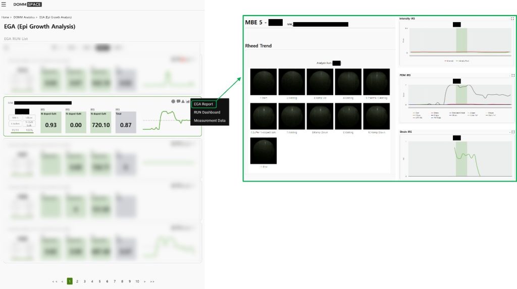
In this n⁺-GaN regrowth, the wafer was patterned with a SiO₂ mask, so the electron diffraction pattern appeared relatively weak. However, it was still sufficient for Domm-ai to perform real-time analysis. Throughout the entire growth process, Domm-ai continuously analyzed the intensity of the electron diffraction pattern, the growth mode (PDM) transitions, and strain variations in real time. Based on this analysis, the system predicted the wafer quality and ultimately recorded a high score of 0.87. Even from Domm’s prediction result alone, it was evident that the selective area growth of n⁺-GaN was successfully completed, and that n⁺-GaN was grown in a 2D mode.
IVWorks leverages its proprietary Hybrid-MBE technology to achieve perfect selective area growth of n⁺-GaN exclusively in the source/drain regions, while maximizing productivity through the Domm-ai system.
The n⁺-GaN regrowth requested by the customer was successfully completed using IVWorks’ Hybrid-MBE and regrowth technology. Perfect selective area growth was achieved, with no growth observed on the masked regions, and n⁺-GaN was grown only in the source/drain regions to a target thickness of 80㎚, maintaining 2D-mode growth for proper epitaxial contact with the 2DEG sidewalls. Even on the fine steps formed at the interface between the SiO₂ mask and the etched regions, the n⁺-GaN layer grew smoothly and uniformly, ensuring complete coverage.

To ensure uniform n⁺-GaN regrowth across the full 6-inch wafer, multiple locations on the wafer were precisely measured by position. We are now preparing packaging for delivery to the customer, following this verification.

The wafer, with n⁺-GaN selectively regrown in the source/drain regions of a 6-inch GaN HEMT on Si, has been vacuum sealed and successfully shipped to the customer. IVWorks’ n⁺-GaN regrowth service supports wafer sizes from 2 inches to 12 inches, and is compatible with GaN HEMT structures on Si, SiC, GaN and Sapphire.
Inquiries │IVWorks Website QNA or www.domm.ai/contact
news
We’ve received a process order for n⁺-GaN regrowth from a university in Asia. IVWorks offers a special epitaxy service that enables selective-area growth of n⁺-GaN in the Source/Drain regions at temperatures as low as 700°C. This process allows non-annealed ohmic contact—without the need for RTA of ohmic metals—and achieves contact resistivity below 0.1 Ω·mm.
IVWorks responds swiftly not only to corporate customers but also to small-volume process requests from university research labs. You can now design a wide range of epitaxial structures—including n⁺-GaN regrowth and p-GaN regrowth—and get instant quotes in real time at www.domm.ai/epidesign.
At IVWorks, when we receive patterned wafers from customers, the first step is to inspect the etched surfaces of the Source/Drain regions—where selective regrowth will take place—using SEM measurements.
Can n+-GaN Regrowth on a Rough Etched Surface?
The patterned wafers we received for this order used SiO₂ as the mask material. Both SiO₂ and SiN are ideal mask materials for IVWorks’ selective area regrowth process—no growth occurs on the masked regions, and n⁺-GaN is grown exclusively in the Source/Drain areas.
For this customer, the etched surface of the Source/Drain regions appears rougher than those from other clients. Since etching processes vary by customer, surface conditions can differ from wafer to wafer. To minimize the impact of surface roughness, IVWorks applies initial growth conditions optimized for surface recovery at the beginning of the regrowth process.
In our experience, as long as mask material residues (SiO₂ or SiN) are not left on the etched areas, surface recovery is generally achievable.
Before performing n⁺-GaN regrowth on customer wafers, IVWorks grows an n-GaN test wafer using the same substrate material and wafer diameter as the customer’s, under identical growth conditions intended for the final regrowth. This step allows us to verify the n-type doping properties in advance, ensuring exceptional accuracy and reliability in the actual regrowth process.
Using a 4-inch SI-SiC wafer, identical to the patterned wafers provided by the customer, we successfully grew an n-GaN test layer and confirmed both the precise growth rate and the n-type doping properties. A doping concentration of 1.26 × 1020 cm⁻³ was achieved, confirming sufficient doping levels. Based on these results, we are proceeding with the regrowth on the customer’s patterned wafers under the same conditions.
IVWorks grows n⁺-GaN using its proprietary Hybrid-MBE system. Now in its 4th generation, the Hybrid-MBE platform supports n⁺-GaN regrowth on wafers ranging from 2-inch to 12-inch diameters.
The Hybrid-MBE system developed by IVWorks is capable of using both N₂ plasma and NH₃ gas injection as nitrogen sources. Using N₂ plasma enables direct supply of atomic nitrogen, allowing precise control over the V/III ratio and minimizing hydrogen incorporation in the film, since no hydrogen byproducts are generated. However, due to the limited efficiency of atomic nitrogen generation, growth rates are relatively low, and it is challenging to ensure uniformity across large wafer areas.
In contrast, NH₃ gas injection allows for high-volume nitrogen delivery with excellent spatial uniformity, enabling faster growth rates under N-rich conditions and supporting uniform III-N film growth even on large-diameter wafers. One of the greatest advantages of NH₃-based growth in IVWorks’ Hybrid-MBE system is its ability to achieve perfect selective area growth.
With perfect selective area growth of n⁺-GaN only in the Source/Drain regions, IVWorks’ Hybrid-MBE significantly simplifies downstream processing for customers—making it one of the most powerful and enabling technologies available.
Although the etched regions of the patterned wafer provided by the customer were relatively rough, IVWorks successfully achieved perfect n⁺-GaN regrowth using its Hybrid-MBE and regrowth technology. Selective area growth was fully realized—no growth occurred on the mask regions, and n⁺-GaN was grown only in the Source/Drain areas. The regrown n⁺-GaN layer, precisely 80 nm thick, was grown in 2D mode, ensuring epitaxial contact with the 2DEG sidewalls.

To ensure uniformity, multiple locations across the 4-inch wafer—after n⁺-GaN regrowth—were precisely measured. With the results verified, we are now preparing the packaging for delivery to the customer.
The 4-inch GaN HEMT on SiC wafer with n⁺-GaN selectively regrown in the Source/Drain regions has been vacuum-packed and shipped to the customer. IVWorks’ n⁺-GaN regrowth service supports wafer sizes from 2 inches to 12 inches, and is compatible with GaN HEMT structures on Si, SiC, and Sapphire.
Inquiries │IVWorks Website QNA or www.domm.ai/contact
news
Semiconductor manufacturing is a highly complex and precision-driven industry, requiring the expert judgment and meticulous control of skilled engineers. Our company has recently launched an AI-based production automation service—MBE Run Automation—through our proprietary artificial intelligence platform, DOMM. This service integrates an AI model capable of analysis and decision-making with existing equipment control systems, automating key tasks previously handled by fab engineers. The solution is already contributing to increased productivity and cost reduction, and is particularly well-suited to large-scale manufacturing environments thanks to a software architecture that scales flexibly with the number of fabs and equipment units. This article presents real-world examples of how this technology is being implemented in actual production settings, and how AI agents are evolving within the semiconductor manufacturing domain at IVWorks.
1. From Fab Engineers to AI-Driven Systems
The global manufacturing industry is undergoing an unprecedented transformation. Just as humanoid robots and smart factories are being adopted in automotive assembly lines, semiconductor manufacturing is also witnessing an expansion of AI technologies into increasingly complex and precise process domains. Our company specializes in epitaxial wafer production—a core semiconductor process that involves the atomic-level deposition and growth of single-crystal thin films on substrates.
This process directly impacts the performance and reliability of next-generation devices such as LEDs, laser diodes, RF components, and power semiconductors. With deep domain expertise and extensive hands-on experience, we have developed our proprietary AI platform, DOMM. While initial development focused on data analysis and process modeling grounded in process interpretation, we have recently introduced the DOMM Agent, a production automation AI agent capable of making real-time decisions and executing tasks autonomously on behalf of engineers.
2. Tracing the Actual Production Flow of Epitaxial Growth
The semiconductor manufacturing process of producing—or more precisely, growing—epitaxial wafers follows a sequential and cumulative flow that begins with initial substrate preparation, continues through thin-film growth, and extends to the subsequent processing stages. Any failure—whether during the wafer loading/unloading process that transfers the substrate into the main chamber, in preparing optimal conditions for thin-film growth, in the atomic-scale stacking of crystalline layers, or in controlling interlayer strain—can critically affect final product quality. Therefore, precise analysis and real-time monitoring at every step of the process are especially crucial for ensuring productivity and quality. The DOMM Agent provides integrated control across this production flow and autonomously performs related mechanical operations such as wafer loading/unloading and chamber state initialization.
For example, it responds in real time to various scenarios such as halting and re-aligning upon detection of misalignment during wafer loading, identifying wafer ID mismatches, issuing alerts in case of vacuum stabilization failure, or initiating a system shutdown if an anomaly is detected in the source shutter. Logs collected at each process stage are analyzed and reflected in subsequent task executions, enabling continuous process optimization through iterative learning. The DOMM Agent also analyzes key data in real time—such as chamber conditions before and after growth, temperature history, and RHEED pattern logs—and utilizes these data to predict product quality and perform operations accordingly.


3. AI Operators: Gaining a Deeper Understanding of Epitaxial Thin-Film Growth
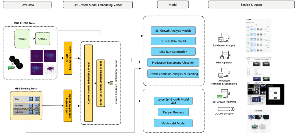
MBE (Molecular Beam Epitaxy) is a high-precision process essential for producing next-generation devices such as power semiconductors, high-frequency components, and quantum devices—but it also demands extensive expertise and experience. This process allows real-time observation of atomic-scale surface formation using RHEED (Reflection High-Energy Electron Diffraction). Recognizing the critical importance and potential of RHEED data for AI-driven approaches, we have developed a range of analytical models based on it. RHEED patterns are obtained through electron beam diffraction and appear as images on a screen representing the reciprocal lattice space of the thin-film surface. These patterns enable real-time identification of crystal growth modes—such as 2D, 3D, or amorphous structures—as well as surface flatness, crystallinity, and changes in lattice spacing, making RHEED an essential data source for in-process condition analysis.
For instance, one of our Epi Growth Analysis Models—based on RHEED pattern detection—offers real-time individual and comparative analysis services, playing a significant role in both product development and production by evaluating thin-film conditions across different time points. However, there have been limitations in interpreting the complex, sequential growth behavior of this time-series data in a higher-dimensional context. Because semiconductor thin-film growth is a continuous and intricate process from the substrate stage to completion, a more sophisticated approach to time-series analysis and modeling is required for deeper understanding and control. To address this, we developed ARHEED—a high-dimensional embedding format for RHEED data—and subsequently built a transformer-based Large EPI Growth Model to enable integrated understanding of physical growth conditions and empirical data. By embedding the entire sequence of EPI growth conditions, this model significantly enhances the interpretive and decision-making capabilities of the AI Agent.
4. AI That Complements Human Engineers
The DOMM Agent is designed not just to automate repetitive tasks, but to emulate the intuition and judgment of skilled engineers based on data, enabling it to directly control the MBE equipment’s control PC. By simply registering a schedule in DOMM Space (DOMM’s production portal), it can carry out tasks even during nights and holidays, analyzing the status of epitaxial growth in real time and assessing equipment control conditions to proceed accordingly. As a result, fab engineers are freed from repetitive monitoring and adjustment tasks, allowing them to focus on higher-value research and development. This also enables a single engineer to manage more equipment simultaneously, improving both manpower efficiency and production cost-effectiveness.
5. Multiple AI Agents with Diverse Roles for Deeper Understanding of Epitaxial Wafer Production
The introduction of the DOMM platform and its foundational AI agents presents a new paradigm for applying AI in semiconductor manufacturing. We have successfully developed and deployed a production automation AI agent capable of directly operating the control PC, achieving meaningful results in understanding the process deeply and making autonomous decisions and executions. In addition, research on LLM-based decoders and multimodal models is currently underway. These models are expected to be integrated into future AI agents, further enhancing precision, quality stability, and productivity—potentially surpassing human engineers.
The focus is no longer on AI that merely analyzes and visualizes data, but on developing and operating role-specific AI agents that understand the process, make their own decisions, and execute appropriate actions. When these agents collaborate organically, the precision and efficiency of semiconductor manufacturing will be significantly improved. These real-world systems and use cases represent an important milestone in the evolution of intelligent manufacturing platforms in the semiconductor industry.
Hong-Kyun Noh ㅣ Artificial Intelligence Team leader & CIO at IVWorks
“We spread values of data”
news
Editor’s Note : This post is the first in a three-part series titled “How AI-Agents Are Transforming the Materials Ecosystem.” Before I introduce IVWorks’ DOMM AI-Agents, I would like to first help you understand the general concept of AI-Agents and the relationship between companies and these agents.
Rather than focusing on technical details, this series emphasizes insights, serving as a prelude to deepen your understanding when you encounter future technical columns. If you have any questions, please feel free to leave a comment. I hope you look forward to and support IVWorks’ AI research!
The Continuing AI Craze
Over the past few days, there has been a surge of interest in Ghibli-style images.
As ChatGPT began generating images in specific artistic styles, many users created their own versions of “Ghibli worlds” with ease. Without needing to issue detailed instructions, a simple request would be enough for the AI to understand user intentions, making the process highly convenient. As this trend started to fade, a new one quickly emerged: users began expressing themselves in a Barbiecore style, resembling toy figurines. Although the hype around particular filters has lessened, AI-based trends have firmly taken root across social media. Despite critical voices raising concerns about the value of creativity and copyright issues, ChatGPT became the most downloaded mobile app in the world last March.

However, AI is no longer just about transforming photos.
It is now evolving into AI-Agents that can understand user goals and take action on their own. Last month, Amazon—the world’s largest e-commerce company—unveiled its next-generation AI-Agent model, “Nova Act.” According to their description, this model is capable of moving beyond simple repetitive tasks and even identifying users’ hidden needs and preferences. Following the release of Nova Act, numerous articles analyzing the competitive landscape among Big Tech companies were published. This highlighted the increasingly intense race within the AI-Agent market. Today, an animation style that once took 30 years to develop can be recreated in just 30 seconds. Every morning, we wake up to a flood of new tools and open-source projects. Along with the wider accessibility of AI technology, the rapid cycle of AI industry trends—where new innovations emerge and fade at astonishing speed—is becoming ever more pronounced. In this landscape, where both Big Tech giants and startups alike are racing to secure technological leadership, one key question arises: What exactly are AI-Agents?
“AI has rapidly advanced from perception AI to generative AI, enabling us to understand and create images, text, and sounds. Now, we have a generative AI that can process, reason, plan, and act. n the future, AI agents will act as a digital workforce, collaborating with employees and performing tasks.” – CES 2025 — Keynote by Jensen Huang, Founder and CEO of NVIDIA
How Are AI-Agents Different?
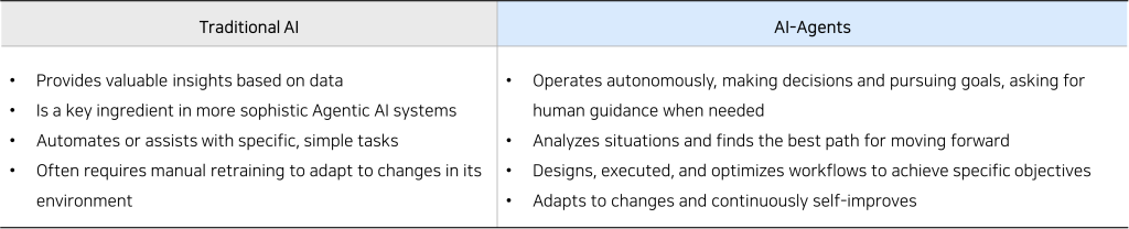
AI-Agents are entities endowed with autonomy and authority.
Freedom and authority for a computer? It might sound a bit strange. In this context, “autonomy” means the AI can operate and make decisions independently without continuous human intervention. “Authority” refers to the power granted by humans to perform certain tasks. In other words, when given an appropriate goal, an AI-Agent can act independently without human involvement. It can design, execute, and optimize a workflow on its own. Therefore, to truly be considered an AI-Agent, it must be capable of performing the three functions of “perception,” “decision-making,” and “action” by itself.
When we compare conventional AI with AI-Agents, we find that although they are closely related, there are important conceptual differences. Traditional AI is more akin to a “tool” that performs specific tasks. In contrast, an AI-Agent interacts with its environment, making its own decisions and taking actions to achieve its objectives—thus encompassing traditional AI within its broader framework.
Reference : What’s the difference between agentic AI and traditional AI?
This brings up an important question: To what extent can we define something as an AI-Agent?
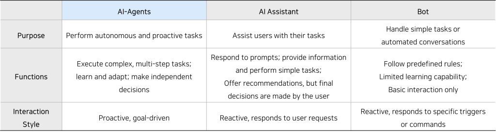
Many people equate AI-Agents with assistants and bots, viewing them all as intelligent automation systems. An AI assistant understands user requests, provides information, and helps perform tasks, much like a secretary. An AI-Agent, however, is more proactive—acting like a strategist that identifies the optimal solution and carries it out.

Let’s take the example of financial services. A bot can automatically respond to customer inquiries such as, “What are your business hours?” or “How can I open an account?” An AI assistant helps bank employees by handling tasks like balance inquiries, fraud alerts, and loan applications. It can also support secure financial management by providing personalized advice based on the customer’s spending habits. An AI-Agent, on the other hand, monitors real-time transaction activities and detects suspicious behaviors. If any anomalies are found, it can proactively block the threat before it spreads, thus preventing fraud in advance. In addition, it can adjust security protocols, refine risk models, and even analyze market trends to autonomously execute trades.
Reference : AI agents vs. AI assistants, Cloud What is an AI agent?
How AI-Agents Handle Requirements
Advanced AI-Agents are not merely input-output systems; they possess autonomous intelligence systems capable of interacting with their environments, making judgments, learning, and taking actions.How exactly do AI-Agents receive, process, and act on external information?
[Inputs from the External World: User Inputs and Environment]
At their core, AI-Agents operate based on responses to their external environments.These inputs can be broadly categorized into two types:
1. User Input: External signals that trigger the AI-Agent’s operation.
2. Environment: The domain within which the AI-Agent operates.
· Digital Infrastructure: Digital spaces such as the web, software, databases, APIs, etc.
· Physical Infrastructure: Spaces connected to the real world, such as robots, sensors, and IoT devices.
[Perception Interface: Sensors]
Sensors collect and detect information from the external world.They accept a wide range of inputs—including user commands, web data, images, and audio—and refine and transform this information into formats that internal systems can understand.This is more than simple data reception; it is the first step in converting external stimuli into meaningful internal data.
1. Sensors: Mechanisms through which AI-Agents perceive their environment.
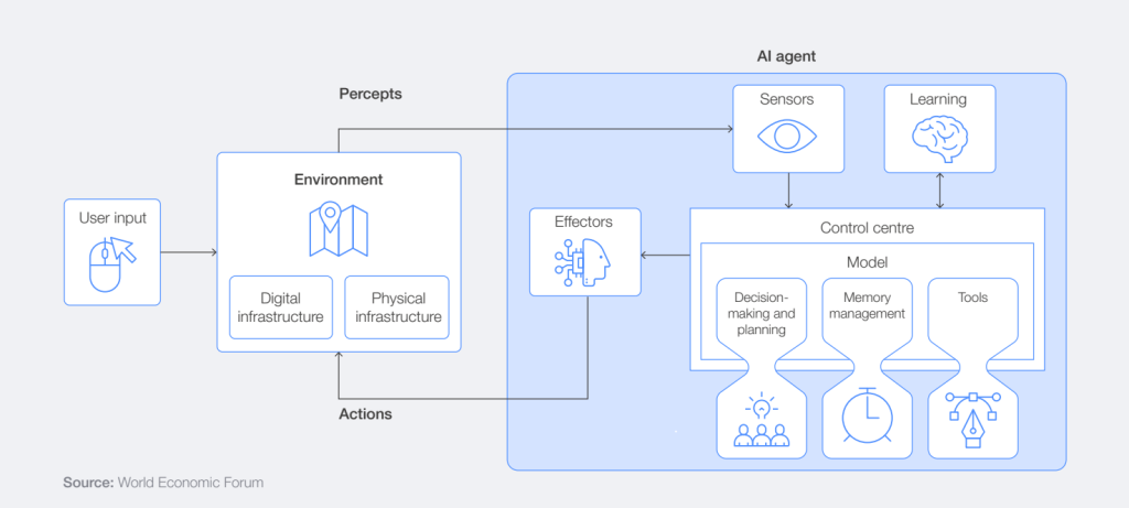
[Internal Processing and Execution: Control Center, Models, Execution, Learning]
Data gathered through sensors is passed into the AI-Agent’s internal systems, where true intelligence comes into play.This area is composed of various functional blocks, each interconnected to generate meaningful behaviors and responses.
1. Control Center: Oversees the flow of information and operations within the AI-Agent.
· Models: Carry out tasks such as reasoning, generation, judgment, and response.
– Planning and Decision-Making: Solve complex tasks through multi-step reasoning and planning logic.
– Memory Management: Retain conversation history, context, and user information to enable consistent and coherent -decision-making.
– Tools: Extend functionalities by invoking external tools such as web search, calculators, database queries, and external APIs.
2. Effectors: Execute actual behaviors or provide feedback to users.
3. Learning: Update the system based on performance results, feedback, and failure cases.
Following is a hypothetical conversation between an AI-Agent and a user, illustrating how the architecture described above is reflected in practice:
👩 : I’m thinking of buying a laptop on Amazon.
🤖 : What kind of laptop are you looking for? If you tell me your budget, preferred brand, and desired features, I’ll recommend the best options.
👩 : My budget is under 700 dollars, and I’d prefer a 15-inch screen.
🤖 : Got it. I’ll search for 15-inch laptops under 700 dollars.
(AI-Agents searches Amazon for laptops…)
(Analyzing price, specs, and user reviews…)
🤖 : Here are some recommendations!
First, a 15-inch laptop from Brand A: priced at 650 dollars, 16GB RAM, 10-hour battery life, rating 4.5 stars.
Second, a 15.6-inch laptop from Brand B: priced at 690 dollars, 8GB RAM, ultra-light design, rating 4.8 stars.
Third, a 15.5-inch laptop from Brand C: priced at 620 dollars, 16GB RAM, high-resolution display, rating 4.3 stars. Which one do you prefer?
👩 : Which one has the most reviews?
🤖 : Brand B has the most reviews. It’s priced at 690 dollars, has 8GB RAM, an ultra-light design, a 4.8-star rating, and over 2,000 reviews.
👩 : Sounds good! I’ll go with the Brand B laptop.
🤖 : Excellent choice! (Adding to cart and proceeding to checkout…)Please select a payment method:
1. Use existing card, 2. Add a new card, 3. Choose another payment method.
👩 : I’ll use my existing card.
🤖 : Confirmed. Shall I use the saved shipping address (123 Teheran-ro, Gangnam-gu, Seoul)?
👩 : Yes.
(AI-Agent processes the payment···)
🤖 : Your purchase is complete! The estimated delivery date is in 3 days. An order confirmation has been sent to your email.
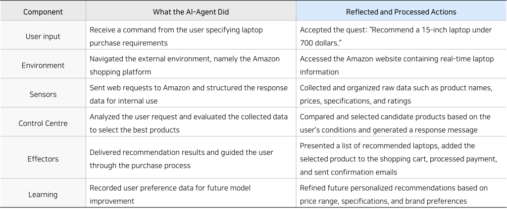
Although this example focused on a shopping scenario, AI-Agents are capable of performing a wide range of tasks. Some AI-Agents specialize in search operations, while others excel at personalized recommendations. At times, multiple AI-Agents collaborate to deliver even more powerful capabilities. In this sense, AI-Agents can each have their own specialized domains of expertise.
Different Perspectives on AI-Agents
AI-Agents are intelligent systems that autonomously analyze their environments and achieve given objectives. They can be deployed across various industries for tasks such as automating workflows, optimizing processes, and delivering personalized services. However, they also have their limitations. For example, while AI-Agents excel in dynamic environments and complex decision-making, achieving such capabilities requires sophisticated programming and high-quality data.
From a Technological Perspective
· Improved Efficiency : Many organizations suffer from operational bottlenecks and human errors caused by repetitive and mundane tasks. AI-Agents can restructure these tasks independently, enabling real-time decision-making and automating workflows. This not only reduces operational costs but also allows human resources to focus on higher-value activities.
· Data-Driven Decision-Making : When data volumes become massive, making timely, informed decisions becomes difficult. AI-Agents can collect and process vast amounts of real-time data to provide clear, evidence-based insights, enabling faster, data-driven decision-making. However, their effectiveness heavily depends on the quality of the underlying data, making robust data management essential.
· High Technological Barrier : Building AI-Agents goes far beyond creating simple chatbots; it involves integrating perception, reasoning, and action. This requires deep expertise in agent architectures, LLM configuration, prompt engineering, API integration, and state management mechanisms. Additionally, the current ecosystem lacks comprehensive technical guidance for building and deploying such agents effectively.
· Security Risks : AI-Agents must contend with emerging security threats. Malicious actors might retrain models to embed harmful code or contaminate them with false information. Although countermeasures such as security logging, input validation, and AI firewalls are evolving, a comprehensive, real-time security infrastructure is urgently needed.

From a Socioeconomic Perspective
· Cost Reduction : High operational costs can severely impact corporate profitability. AI-Agents help reduce inefficiencies and human error-related costs, boosting overall productivity and enabling more agile business operations.
· Personalized Services : By analyzing purchasing history, behavioral patterns, and real-time feedback, AI-Agents can offer personalized product recommendations and customer interactions. This strengthens brand loyalty and improves conversion rates.
· Impact on Employment :The adoption of AI-Agents could alter existing job structures, with repetitive and rule-based jobs increasingly automated. Workforce reskilling and job redesign must be considered to mitigate the socioeconomic impact.
· High Initial Implementation Costs : Deploying AI-Agents requires substantial initial investments in infrastructure and cybersecurity measures. Ongoing maintenance costs must also be factored in, making the financial burden significant for companies considering adoption.
From an Ethical Perspective
· Lack of Decision-Making Transparency : AI-Agents often lack ethical judgment and operate like “black boxes,” making it difficult for users to understand how decisions are made. This opacity raises concerns about potential errors or biases embedded in the decision-making process.
Reference : AI Agents: Definition, Types, Benefits & Use Cases, 생성형 AI 에이전트 ‘에이전틱 AI’에 거는 기대
AI-Agents in the Semiconductor Materials Industry
Given the complexity of decision-making and the real-time control demands in industrial settings, AI-Agents present a compelling solution. Particularly in precision-driven fields where data-centric operations are crucial, AI-Agents can eliminate bottlenecks and inefficiencies that traditional systems struggle with. One prime example is the semiconductor industry. The semiconductor sector is characterized by highly complex processes, diverse equipment, and strict quality standards. Within this sector, the materials segment — the foundational layer of the industry — remains relatively less automated and heavily reliant on human expertise. Compound semiconductors, such as gallium nitride (GaN), are particularly challenging due to their intricate manufacturing processes. GaN epitaxy (epitaxial growth) — a critical step in producing next-generation semiconductors that could replace silicon — demands extreme precision, substantial resources, and extensive time investments for mass production optimization. As such, GaN epitaxy materials represent an ideal domain where the full potential of AI-Agents can be unleashed.
Why Now for AI-Agents?
1. Industrial Transformation and Timing for AI-Agent Adoption
The compound semiconductor market, including GaN, underpins future industries like fast-charging technologies, aerospace, 5G, and electric vehicles due to its high-frequency, high-power, and high-efficiency characteristics. Success in these fields depends not just on technical prowess but on how quickly and flexibly companies can respond to changing demands. Today’s material industry competition extends beyond manufacturing — supply chain resilience, operational agility, and customer-specific technology adoption have become critical success factors. Amid global supply chain disruptions driven by political and economic variables, companies need both technological strength and operational excellence. AI-Agents can act as a strategic lever for transformation in this context.
2. Shift from Traditional Manufacturing to Intelligent Operations
Traditionally, compound semiconductor material manufacturing relied heavily on skilled human expertise and incremental optimization through manual adjustments. However, the current market demands faster response times, adaptive experimentation, and real-time adjustment of complex production conditions. Instead of searching for a single “correct” answer, the new paradigm demands rapid experimentation of valid combinations and immediate operationalization. AI-Agents can digitize and intelligently optimize this approach, making what was once unachievable now possible.
3. Evolving Corporate Strategy Toward AI-Agents
Having experienced gradual AI adoption through chatbots, RPA, and other technologies, companies now recognize AI not merely as a tool but as a strategic operational partner. AI-Agents are no longer just assistants; they autonomously formulate production plans, complete analytical reports, and manage material inventory, connecting entire organizations organically. This shift enables companies to transition from human-centric to intelligence-centric hybrid operating systems, enhancing development speed, customer responsiveness, and creative workforce engagement, while generating new insights from manufacturing data.

Why IVWorks Is Taking the Lead with AI Agents
The compound semiconductor materials industry now stands at the starting point of a major “transition.” In particular, as demand is expanding rapidly, productivity, quality control, and internalization of core technologies must keep pace—yet this remains a significant challenge. Simple mechanical automation technologies alone can no longer overcome the limits of yield and mass production optimization. This is especially true in fields like gallium nitride (GaN), where there are few prior technological precedents; uncertainty in processes and variation in operation based on experience cannot be easily resolved.
In this context, competition in AI agents is intensifying, and manufacturing has finally reached the point where “acting AI” can become a true collaborator. However, applying AI agents to specialized processes—such as those at IVWorks—is extremely complex and challenging. In a domain where process variables and equipment interactions are highly intricate, operating AI systems in the real world is difficult without deep domain expertise. Moreover, what we need is not an all-purpose AI that can answer every question in the world, but an agent that excels specifically in epitaxy.
This is where IVWorks’ role becomes clear. We have been conducting long-term research, technology development, and mass production optimization in the field of gallium nitride epitaxy. We possess a vast amount of internal data accumulated over more than a decade, covering process environments and experimental results. In addition, we have the human resources and technological capability to design and prototype AI agents in-house. Our homemade equipment technology also allows for a high degree of customization, with few limitations. These are differentiating factors that most materials companies lack, and they represent optimal conditions for AI agent design, training, and validation. In other words, IVWorks is not merely a passive adopter of technology, but actively participates in the field of gallium nitride materials as both an AI “architect” and a “builder.”

IVWorks’ AI agent is a concept that integrates and expands various automation elements and intelligent capabilities required for epitaxial growth. In the DOMM AI Agent system, specialized agents are deployed according to specific categories required for epi production—for example, Agent A operates the equipment directly, Agent B manages production scheduling, and Agent C orchestrates the actions of other agents. These agents are organically connected to form an optimized epi-wafer production system.
AI researchers and engineers are supplying and developing the necessary components—such as data, parts, and models—for each agent and are sequentially applying these agents to mass production equipment one by one. Most recently, an agent capable of preparing and initiating a run (equipment operation) without the need for human engineers has been successfully applied, significantly improving the overall completion level of the DOMM AI Agent system.
IVWorks has designed the DOMM AI Agent around the following core principles, ensuring it functions as a part of a mass production system that enhances the company’s overall productivity:
· End-to-End Optimization : Capable of being involved in the entire flow—from structure design, recipe generation, and production, to analysis and learning.
· Collaboration-Centric Design : A platform that allows engineers to jointly design and share across different equipment and processes.
· Explainable Decision-Making : Transparent design that allows engineers to understand the basis of decisions (e.g., past runs, measurement values).
· Agent Internalization : A framework for developing and advancing agents independently, without relying on tools from specific vendors.
So far, we have explored the concept, structure, advantages, and limitations of AI agents, as well as the reasons why their adoption is necessary in the extremely complex domain of semiconductor materials. As AI agent implementation continues to progress, IVWorks’ DOMM AI Agent is approaching its final stage of completion. In the next installment, we will take a closer look at how IVWorks has built its AI agent system, comparing it to traditional methods of epi production, and examine how it is being utilized from the perspective of the producer.
Yoon-Seo Cho l Marketing Assistant at IVWorks
※This article reflects the subjective opinions of the contributor and may differ from the official position of IVWorks
news

When I was a kid, there was an arcade game where I had to rapidly press red, yellow, and blue buttons. The faster I pressed, the faster my character would run. But since the opponent was always a computer, no matter how frantically I hit the buttons, I could never win. Of course, there was no way a human could beat a program, but I still remember the hollow feeling of looking at my reddened hands and wondering if my actions were really that slow.
In the blink of an eye—just one second—a power semiconductor performs over 1,000 switching operations. During this process, it converts electrical energy, altering voltage, current, frequency, and the form of electricity (AC/DC). The faster the switching operation, the higher the speed and precision of electrical signal conversion, enabling more efficient power conversion.
About 95% of power semiconductors are made from silicon (Si). It is inexpensive, easy to control in terms of electrical conductivity and structural form, and has essentially become the standard semiconductor material. However, as high-value industries such as electric vehicles, power grids, 5G infrastructure, and industrial automation continue to accelerate, extreme levels of efficiency in high voltage, high current, and high power applications have become crucial. With Si reaching its physical limits, GaN (gallium nitride) and SiC (silicon carbide) have emerged as the most promising alternatives, while materials such as Ga₂O₃ (gallium oxide) and AlN (aluminum nitride) are also following suit.
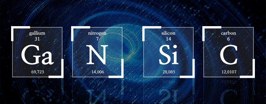
Si (Silicon) has a high coefficient of thermal expansion, making it less stable and durable in high-temperature environments. As a result, when the temperature exceeds approximately 150°C, it loses its semiconductor properties. SiC was developed to address this limitation by bonding carbon (C) to silicon in a 1:1 ratio. It is physically and chemically highly stable and extremely hard. On the Mohs hardness scale, where diamond ranks at 10, SiC falls between 9.2 and 9.3. Unlike Si, it retains its semiconductor properties regardless of temperature and has a breakdown voltage 10 times higher than that of Si (0.3 MV/cm). This allows semiconductors to function properly even under high voltage without performance degradation. GaN is a compound composed of gallium (Ga) and nitrogen (N). It gained prominence in the late 1990s when it was used in blue light-emitting diodes (LEDs). However, due to its high electron mobility, strong breakdown voltage, and excellent thermal conductivity, it is now regarded as the ideal material for RF devices requiring high-frequency efficiency and for fast-charging applications.
One of the key expectations for SiC and GaN in the semiconductor industry is low power loss.
The reason these materials exhibit lower power loss compared to Si lies in their wide bandgap (WBG) properties. The bandgap refers to the gap (distance) between the conduction band and the valence band. Electrons move across this gap, enabling the flow of electrical energy. Every material has a unique bandgap: Si has 1.2 eV, SiC has 3.3 eV, and GaN has 3.4 eV—the highest among them. When energy (in the form of current, heat, etc.) is applied to a material, electrons in the valence band move to the conduction band, which we perceive as “current flow.” However, if the bandgap is too wide (above 4 eV), it becomes difficult for electrons to reach the conduction band. This is why materials with bandgaps between 0.1 eV and 4 eV are classified as semiconductors, while those with even larger bandgaps are considered insulators.
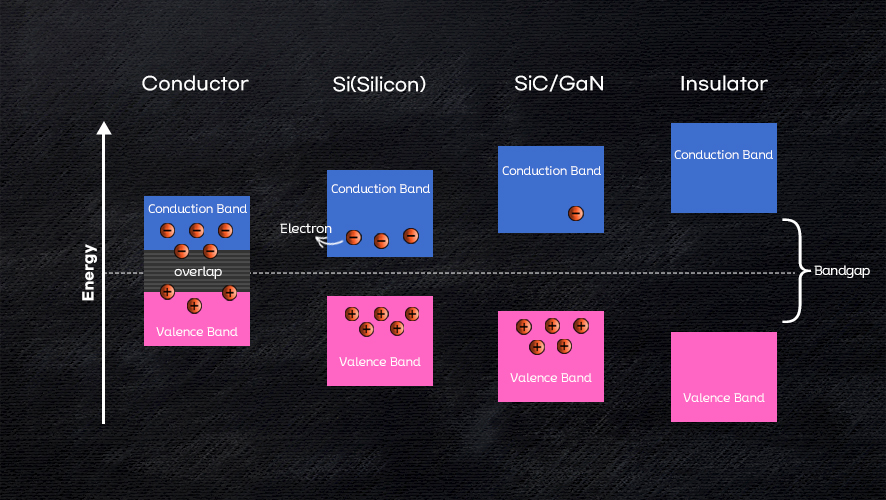
If the bandgap is narrow, electrons can more easily reach the conduction band. Electrons that reach the conduction band become “free electrons,” capable of moving freely. In other words, a narrower bandgap leads to more free electron generation. As the electron movement increases, frequent collisions with the lattice generate thermal energy. For instance, if 100W of power is supplied, but 30W is lost as heat, only 70% efficiency is achieved. Furthermore, excessive heat can reduce the mobility of the device or increase leakage current, leading to higher power consumption. On the other hand, when the bandgap is wide, much more energy is required for electrons to reach the conduction band. If there is insufficient energy, most electrons remain in the valence band, reducing the number of free electrons and helping to prevent power loss.
However, when the bandgap is wide, more energy is required, which leads to lower energy efficiency in systems that operate at lower voltages. Therefore, it is primarily used in power semiconductors for high-voltage, high-frequency environments. High-temperature environments tend to narrow the bandgap, so if the bandgap is wide from the start, it can maintain its wide bandgap at high temperatures and control the movement of free electrons. This is why SiC and GaN are referred to as wide bandgap (WBG) semiconductors and are gaining attention as materials suitable for high-frequency, high-voltage, and high-temperature environments.
With these advantages, the global market size for GaN and SiC power semiconductors is predicted to exceed $15 billion by 2032 (global market). Although the period of use is short and they are 2 to 3 times more expensive than Si, making the market size relatively small, governments around the world are moving quickly to build domestic WBG power semiconductor production capabilities, considering the growth of the power semiconductor industry and its importance for national security.
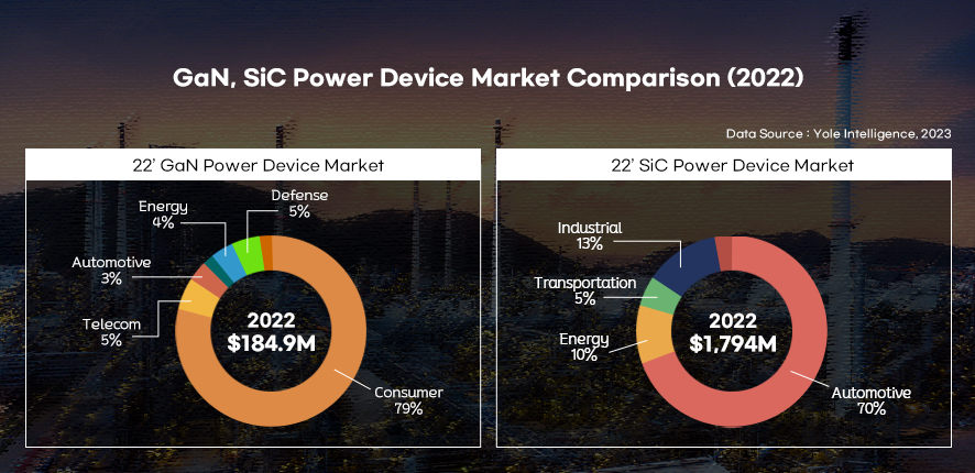
Among the two materials, SiC was the first to gain attention in the power semiconductor market. SiC has long proven its technological reliability in industrial equipment such as power transmission and distribution, industrial inverters, and wind and solar power generation. In particular, the market rapidly expanded as well-known electric vehicle manufacturers began adopting SiC in recent years. An electric vehicle contains about 60 to 80 power semiconductors. Due to the characteristic of having to place high-voltage batteries in a limited space, these semiconductors must withstand ultra-high voltage and extreme heat. Power semiconductors for electric vehicles are responsible for energy conversion and control, and are used in inverters, converters, onboard chargers, and battery management systems. Electric vehicle inverters using SiC power semiconductors are up to 10% more energy-efficient than Si semiconductor inverters, and also reduce volume and weight. By reducing power loss, the vehicle’s weight can also be reduced, making it considered the optimal material for e-mobility. According to data from the French market research firm Yole Group, the SiC power semiconductor market was $1,794 million in 2022, while the GaN power semiconductor market was $184.9 million, clearly showing that the SiC power semiconductor market is significantly larger.
On the other hand, GaN began to be used in the power semiconductor field in earnest from the mid-2000s. Initially, it was mainly used in communication, laser, and LED applications, but as its potential as a power semiconductor started to be gradually recognized, the market has become more active in recent years. The delayed adoption was largely due to technological limitations. Instead of using GaN itself as a substrate, it is typically grown as a thin film on substrates made from other materials such as Si, SiC, or sapphire. However, since two layers with different physical properties need to be grown, the manufacturing difficulty was very high, making it challenging to improve yield. As a result, even when SiC transitioned to large-scale production with 6-8 inch wafers, GaN was still using smaller 4-6 inch wafers.
So, when will the GaN market grow? Although GaN was adopted relatively late in the power semiconductor market, its application range has significantly expanded in recent years. The difficulty in applying the material to production posed challenges for commercialization, but the emergence of specialized epi houses like IVWorks has made the active development of the GaN market possible.

So, is SiC a better material than GaN?
Looking at the electron mobility, which is the characteristic of the movement of electrons that have reached the conduction band, silicon has a mobility of 1,450 cm²/Vs, while GaN has 1,500 cm²/Vs. However, SiC is around 900 cm²/Vs, which makes it less suitable for high-speed switching applications. SiC is harder and has a more complex crystal structure than Si, and due to the strong interaction between electrons and lattice vibrations (phonons), electrons are scattered while moving, resulting in slower movement speeds. Additionally, since the effective mass of SiC is larger than that of Si, the electron movement is relatively sluggish.

When electron mobility is high, fast switching is possible, allowing for efficient power control and high-speed switching in low-power electronic devices. However, as electrons move quickly, collisions and heat generation increase. On the other hand, when electron mobility is low, heat management becomes easier. Additionally, such materials are typically structurally stable, often offering high durability. Therefore, they are advantageous in electronic devices operating in high-temperature or harsh environments (industrial use). However, low switching speeds and limitations on speed and bandwidth can make them less suitable for high-speed communication systems or RF applications.
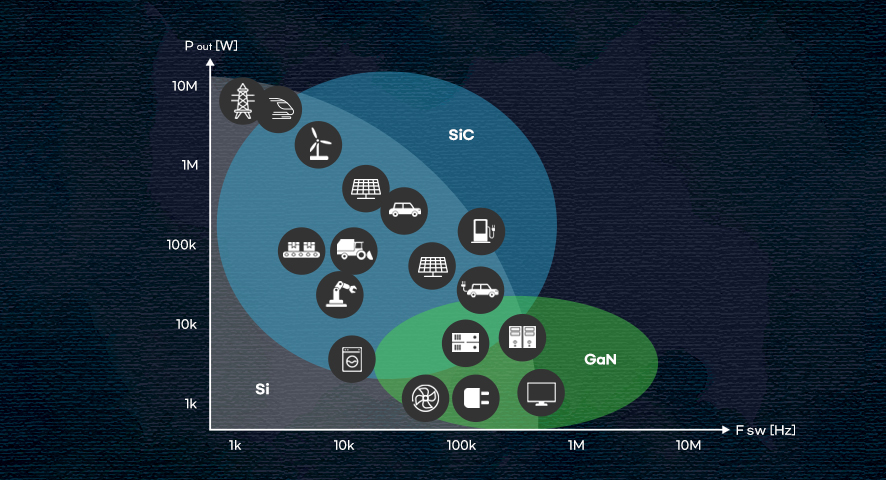
Both materials have a wide bandgap, which reduces power loss and makes them advantageous in high-temperature and high-voltage environments. However, it is difficult to definitively say which material is better. Due to its high electron mobility and fast switching characteristics, GaN is suitable for high-frequency or high-speed communication systems, as well as applications where miniaturization and high efficiency are essential. SiC, on the other hand, excels in systems requiring high temperatures, high voltages, and high durability, making it ideal for electric vehicles, renewable energy systems, and power converters. Depending on the material’s characteristics, specialized applications coexist in the market.
However, the competition between the two materials is not nonexistent. In the medium voltage range of 650 to 1200V, which is primarily used in industrial and high-performance electronic devices, there is potential for substitution, making it a practical competitive arena. This includes electric vehicle onboard chargers (OBC), DC-DC converters, high-speed chargers, and power supply units for 5G base stations. This range represents a transition between low-voltage and high-voltage applications, bridging industrial and consumer markets. As a result, this is one of the most competitive areas in the power semiconductor industry. Therefore, the relationship between the two materials remains a significant point of debate across the industry.
Experts have varying perspectives. However, a common view is that rather than focusing solely on the technical superiority of SiC or GaN, attention should be given to how the strengths of each material are applied to influence future industries. Ultimately, SiC and GaN are expected to play crucial roles in maximizing power efficiency and cost reduction in different applications. How these two materials coexist in the power semiconductor market and how they will meet the technological advancements and market demands will continue to be an important topic of discussion.
Yoon-Seo Cho l Marketing Manager at IVWorks
※This article reflects the subjective opinions of the contributor and may differ from the official position of IVWorks
news
“IVWorks, Maximizing device performance by lowering contact resistance and improving electrical properties through n+-GaN selective regrowth”

In September last year, IVWorks introduced the industry’s first n+-GaN Selective Regrowth service utilizing MBE (Molecular Beam Epitaxy) equipment. This service selectively etches the source and drain areas of GaN epi-wafers. It then precisely regrows n+-GaN to reduce contact resistance, enhance electrical properties, and improve semiconductor device performance.
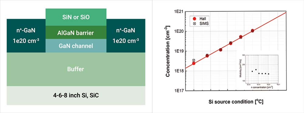
High temperatures during the regrowth process can degrade the quality of the epi-interface, adversely affecting device performance. IVWorks’ Hybrid-MBE process operates in an ultra-high vacuum with minimal impurities. It enables low-temperature processing below 700°C. Additionally, in-situ surface cleaning technology removes impurities from the wafer surface, preventing HEMT device performance degradation during the regrowth process.
| Contact Resistance : Achieves levels as low as ≤ 0.1 Ωmm | |
| Uniformity : 2% or less | |
| High Doping Concentration (n=5.0e19 ~ 2.0e20/cm3) | |
| 2DEG Side-Wall Contact with Regrowth n+GaN Epitaxially | |
| Processing Time : Approximately 2 hours |
Thanks to these technical advantages, IVWorks’ Regrowth service offers exceptional precision and reproducibility in semiconductor device manufacturing.
The n+-GaN Selective Regrowth technology significantly reduces ohmic contact resistance. Resistance can drop to as low as 1/10 of conventional levels, offering superior performance. This reduction minimizes resistance during current flow, significantly decreasing power loss and maximizing device efficiency. Such improvements play a vital role in enabling high-performance device designs and miniaturization.
In particular When applied to RF devices, this technology significantly enhances power efficiency and density. It is particularly valuable in high-frequency environments requiring stable signal processing.
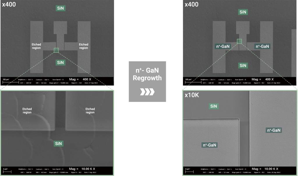
IVWorks’ Regrowth service is compatible with 4-inch, 6-inch, and 8-inch silicon (Si) substrates, as well as 4-inch and 6-inch silicon carbide (SiC) substrates. Its excellent performance has been consistently proven through customer applications. It is highly trusted by leading global semiconductor companies and research institutions.
In February, IVWorks further expanded its offerings by launching the p-GaN Gate Selective Regrowth technology, providing customers with an even broader range of options and reinforcing its technological leadership.
IVWorks’ Selective Regrowth service is available on the WIZDOMM platform (▶https://www.domm.ai/epidesign). Customers can adjust etch depth and mask parameters to design optimized processes. The platform provides instant quotations, saving both time and cost.
Experience the cutting-edge Regrowth technology from IVWorks!
Soo-Jeong Choe l Marketing Assistant Manager at IVWorks
※This article reflects the subjective opinions of the contributor and may differ from the official position of IVWorks