
news
Selective p-GaN Regrowth on 3D FIN Structure of 8″ RF GaN HEMT on Si for a U.S. Customer
We’ve recently received a process order for p-GaN regrowth from a U.S.-based company.
IVWorks specializes in selective area growth services using our proprietary large-scale Hybrid-MBE system, autonomously operated by AI. In addition to GaN HEMT and microLED epiwafers, we support a wide variety of custom regrowth structures. You can design your own epitaxial structures—including p-GaN regrowth and n⁺-GaN regrowth—and get instant quotes directly here.
Just like this project, our ‘p-GaN regrowth’ service enables selective area growth in the Gate region at low temperatures around 700°C—a highly effective solution for implementing normally-off GaN HEMTs. In the rapidly growing communications market, RF-GaN HEMT on Si technology is gaining strong attention—especially for mobile device applications, where minimizing standby power consumption and enabling low-power operation is essential. To achieve this, normally-off RF-GaN HEMT technology is required.
There are two main approaches to implementing normally-off behavior in RF-GaN HEMTs: One is the gate recess method, which thins the barrier layer under the gate through precise etching to suppress 2DEG formation. The other is the p-GaN gate approach, where a p-GaN layer is placed under the gate to deplete the 2DEG channel. The gate recess method, especially when combined with gate length scaling, offers excellent RF performance. However, it comes with challenges in process complexity, threshold voltage stability, uniformity, and typically exhibits higher gate leakage currents.
On the other hand, the p-GaN gate method increases the vertical distance between the gate and the 2DEG due to the thickness of the p-GaN layer, and etching damage can limit aggressive gate scaling—resulting in slightly reduced RF performance. However, this approach allows for simplified processing: the p-GaN layer is grown during epitaxy and patterned to leave the gate region only. With precise control over p-type doping levels and layer thickness during growth, it enables excellent control of threshold voltage characteristics and gate leakage. In summary, the gate recess approach is preferred when maximizing RF performance is the top priority, while the p-GaN gate method is better suited for applications requiring stable normally-off behavior and process simplicity.
IVWorks’ p-GaN regrowth service offers a distinct advantage: since p-GaN is selectively regrown only in the gate region, it eliminates the need for etching the p-GaN layer—avoiding etch-induced damage and enabling the formation of narrow p-GaN gates with improved RF characteristics. In addition, because the regrowth is performed in an ultra-high vacuum MBE chamber, hydrogen compensation in Mg-doped GaN is significantly suppressed. As a result, high hole concentrations can be achieved even with relatively low Mg doping levels, and no additional activation process is required.
The precise growth control offered by MBE also makes it possible to perform regrowth on 3D gate structures, providing further design flexibility.
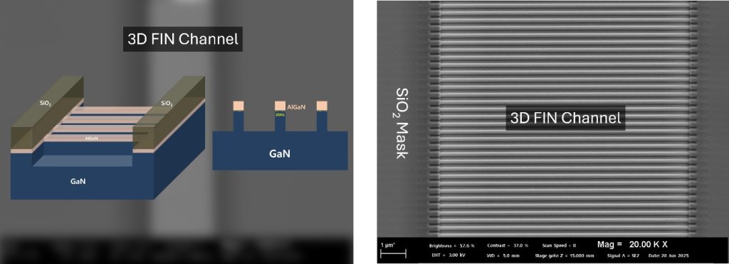
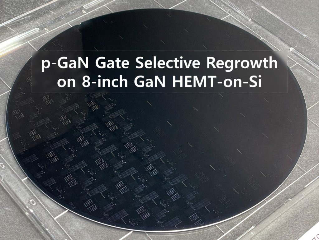
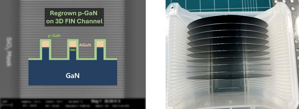
For this project, the customer provided an 8-inch GaN HEMT on Si patterned wafer, with the goal of implementing a final device structure featuring a 3D FIN gate. Accordingly, the selective p-GaN regrowth area was fabricated as a 3D FIN channel structure. The patterned wafer with 3D FIN channels was patterned with SiO₂ as the mask material. Both SiO₂ and SiN are optimal for IVWorks’ selective area regrowth process—no growth occurs on the masked regions, and p-GaN is grown only in the mask-open areas. In this project, the 3D FIN channels were formed as narrow multi-channel structures, with very tight spacing between channels.
Based on our experience at IVWorks, selective area growth is reliably achievable down to ~100㎚, and with sufficiently clean and precise mask etching, we believe growth is possible even at dimensions as small as tens of nanometers—or even just a few nanometers. At IVWorks, before performing p-GaN regrowth on customer wafers, we first grow a p-GaN test wafer using the same substrate material and wafer diameter.
This test is conducted under the exact same growth conditions intended for the final regrowth, allowing us to verify p-type doping conditions in advance—ensuring high process accuracy and reliability for the customer’s wafers.
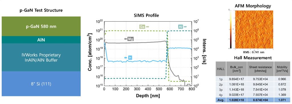
For this project, we grew a p-GaN test structure on an 8-inch Si(111) wafer, identical to the patterned wafers provided by the customer. The p-GaN layer was grown to a thickness of 58㎚ to enable Hall measurements, with an insulating buffer structure grown beneath it on the Si wafer. Growing GaN on a Si substrate is significantly more challenging than on other wafers such as SiC, Sapphire, or free-standing GaN. It requires overcoming lattice mismatch and crystal structure differences between Si and III-nitride films, while precisely managing thermal expansion mismatch, film stress, and maintaining high insulating properties in the buffer layer. Moreover, since direct contact between gallium and the silicon wafer can cause melt-back etching, the system must be carefully operated to prevent any gallium exposure to the Si surface during growth.
To address these challenges, IVWorks applies its patented InAlN/AlN superlattice buffer technology in its GaN-on-Si epitaxy platform. This buffer structure maintains high superlattice bandgap energy for strong insulation, while using the lattice mismatch between InAlN and AlN to precisely control film stress. This platform is highly versatile and can be applied to both RF GaN HEMT on Si and DC power GaN HEMT on Si epitaxial structures.
The growth of the p-GaN test structure confirmed both the accurate growth rate and the desired p-type doping characteristics. SIMS analysis showed a sufficient Mg doping concentration of ~5 × 1019 cm⁻³, and as mentioned earlier, the Hybrid-MBE environment resulted in extremely low hydrogen incorporation. Hall measurements confirmed a hole concentration of 1.0 × 1018 cm⁻³, verifying that the doping levels met the customer’s requirements. Based on this, we proceeded with a 50㎚ p-GaN regrowth on the customer’s patterned wafers under the same growth conditions.
IVWorks grows p-GaN using its proprietary Hybrid-MBE platform, now in its 4th generation, supporting epitaxy services for wafer diameters ranging from 2-inch to 12-inch. Furthermore, IVWorks has established a fully autonomous epitaxy production system by integrating all production processes with Domm, our proprietary AI agent framework.
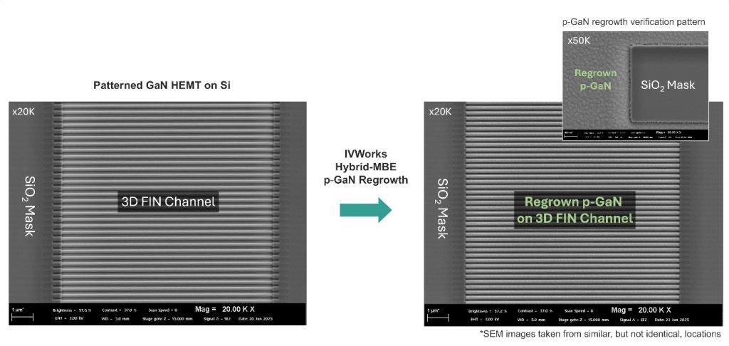
p-GaN regrowth was successfully completed on both the p-GaN gate regions and the selective area growth test patterns of the customer’s patterned wafer. Selective area growth was perfectly realized—no growth occurred on the masked regions, and p-GaN was grown only where intended. The regrown 5㎚ p-GaN layer in the 3D FIN channel regions followed the 3D geometry precisely, forming epitaxial contact on both the sidewalls and top surfaces of the FIN structures.
The wafer, with p-GaN selectively regrown in the 3D FIN channel regions of an 8-inch RF GaN HEMT on Si, has been vacuum-packed and successfully shipped to the customer. IVWorks’ p-GaN regrowth service supports wafer sizes from 2 inches to 12 inches, and is compatible with GaN HEMT structures on Si, SiC, GaN, and Sapphire.
Inquiries │IVWorks Website QNA or www.domm.ai/contact