
news
IVWorks’ n⁺-GaN regrowth service is the optimal choice for customers aiming to realize high-performance GaN HEMTs. It is not only ideal for university research teams pursuing top-level academic results, but also for GaN foundries and IDMs seeking to deliver differentiated device performance to the market. With minimal resource input, IVWorks enables customers to achieve maximum process effectiveness.
This n⁺-GaN regrowth process order was received from an Asian university.
IVWorks performs selective area growth of n⁺-GaN only in the source and drain regions at a low temperature of approximately 700 ℃. This approach can reduce contact resistance(Rc) by nearly one tenth, while enabling non-annealed ohmic contact without the need for RTA of ohmic metals. As a result, it effectively eliminates various degradation issues typically caused by the RTA process.
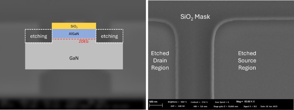
At IVWorks, when we receive patterned wafers from a customer, the first step is to inspect the etched surface of the source and drain regions where selective regrowth is to be performed, using SEM measurements.
The patterned wafer we received for this process was masked using SiO₂. Both SiO₂ and SiN are ideal mask materials for IVWorks’ selective area regrowth, ensuring that no growth occurs in the masked regions. As a result, n⁺-GaN is grown exclusively in the source and drain areas, with complete selectivity maintained after regrowth. The patterned wafer provided by this customer had a very clean etched surface in the source and drain regions, which is expected to allow smooth regrowth.
Although we occasionally receive wafers with rough etched surfaces, IVWorks has established both ex-situ and in-situ cleaning procedures, along with initial growth conditions optimized for surface recovery during the early stage of regrowth. Thanks to these capabilities, surface recovery is generally achievable, and the desired n⁺-GaN properties in the source and drain regions can be reliably obtained.
(*For reference on regrowth over rough etching – 4″ GaN HEMT with n⁺-GaN S/D Selective Regrowth for Asian University)
At IVWorks, before performing n⁺-GaN regrowth on customer wafers, we first grow an n-GaN test wafer using the same material and wafer size as the customer’s, under the exact same growth conditions intended for the regrowth. This allows us to verify the n-type doping characteristics in advance, ensuring a high level of process accuracy. For this particular process, we also developed and applied a modified growth condition at the customer’s request, in order to further increase the n⁺-GaN doping concentration.
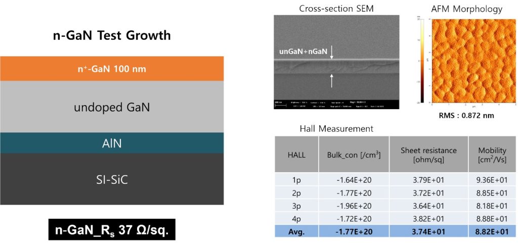
Using a 4-inch SI-SiC wafer identical to the patterned wafer provided by the customer, we applied the newly developed growth condition to perform n-GaN test growth. The results confirmed both the precise growth rate and n-type doping characteristics. A high doping concentration of 1.77×1020 cm⁻³ was achieved, and the sheet resistance was measured at 37ohms/sq, which is approximately half the value obtained under the previous growth condition. Based on these results, we are now proceeding with the growth on the customer’s patterned wafer using this updated condition.
IVWorks grows n⁺-GaN using its proprietary Hybrid-MBE system. Now in its fourth generation, the Hybrid-MBE platform supports n⁺GaN regrowth on wafer sizes ranging from 2 inches to 12 inches. In addition, IVWorks has established a fully autonomous production system by integrating the entire epitaxial wafer production workflow into its proprietary AI agent framework called Domm.
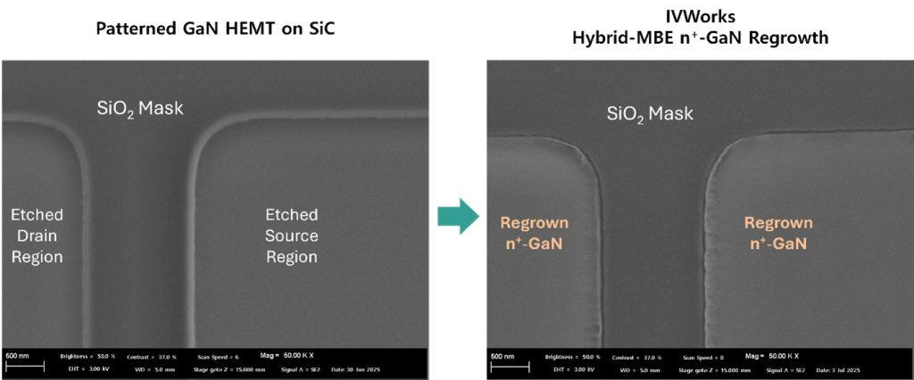
Using IVWorks’ Hybrid-MBE and regrowth technology, n⁺-GaN regrowth was successfully completed on the patterned wafer provided by the customer. Perfect selective area growth was achieved, with no growth observed in the masked regions, and n⁺-GaN was grown only in the source and drain regions. The regrown n⁺-GaN layer reached a thickness of 100㎚, maintained 2D-mode growth, and formed proper epitaxial contact with the 2DEG sidewalls.
The wafer with n⁺-GaN selectively regrown in the source and drain regions of a 4-inch GaN HEMT on SiC has been vacuum sealed and successfully shipped to the customer.
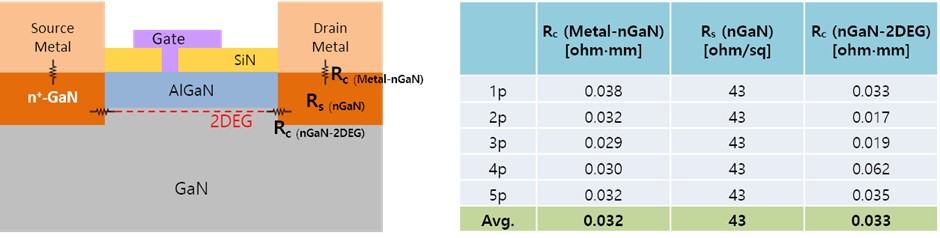
Using the newly developed n⁺-GaN regrowth condition, we observed excellent contact resistance results.
The measured contact resistance between the ohmic metal and n⁺-GaN (Metal to nGaN) was 0.032ohm·mm, and the contact resistance between the n⁺-GaN and 2DEG(nGaN to 2DEG) was 0.033ohm·mm. We received very positive feedback from the customer, who was highly satisfied with these results.
Inquiries │IVWorks Website QNA or www.domm.ai/contact