
news
We’ve received a process order for n⁺-GaN regrowth from a university in Asia. IVWorks offers a special epitaxy service that enables selective-area growth of n⁺-GaN in the Source/Drain regions at temperatures as low as 700°C. This process allows non-annealed ohmic contact—without the need for RTA of ohmic metals—and achieves contact resistivity below 0.1 Ω·mm.
IVWorks responds swiftly not only to corporate customers but also to small-volume process requests from university research labs. You can now design a wide range of epitaxial structures—including n⁺-GaN regrowth and p-GaN regrowth—and get instant quotes in real time at www.domm.ai/epidesign.
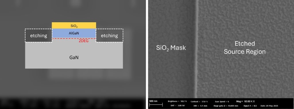
At IVWorks, when we receive patterned wafers from customers, the first step is to inspect the etched surfaces of the Source/Drain regions—where selective regrowth will take place—using SEM measurements.
Can n+-GaN Regrowth on a Rough Etched Surface?
The patterned wafers we received for this order used SiO₂ as the mask material. Both SiO₂ and SiN are ideal mask materials for IVWorks’ selective area regrowth process—no growth occurs on the masked regions, and n⁺-GaN is grown exclusively in the Source/Drain areas.
For this customer, the etched surface of the Source/Drain regions appears rougher than those from other clients. Since etching processes vary by customer, surface conditions can differ from wafer to wafer. To minimize the impact of surface roughness, IVWorks applies initial growth conditions optimized for surface recovery at the beginning of the regrowth process.
In our experience, as long as mask material residues (SiO₂ or SiN) are not left on the etched areas, surface recovery is generally achievable.
Before performing n⁺-GaN regrowth on customer wafers, IVWorks grows an n-GaN test wafer using the same substrate material and wafer diameter as the customer’s, under identical growth conditions intended for the final regrowth. This step allows us to verify the n-type doping properties in advance, ensuring exceptional accuracy and reliability in the actual regrowth process.
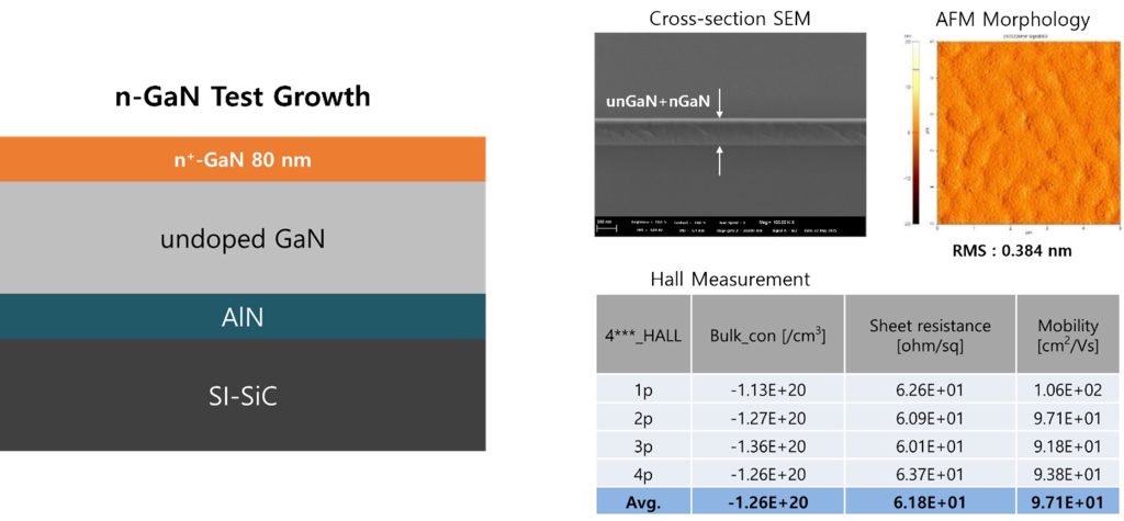
Using a 4-inch SI-SiC wafer, identical to the patterned wafers provided by the customer, we successfully grew an n-GaN test layer and confirmed both the precise growth rate and the n-type doping properties. A doping concentration of 1.26 × 1020 cm⁻³ was achieved, confirming sufficient doping levels. Based on these results, we are proceeding with the regrowth on the customer’s patterned wafers under the same conditions.
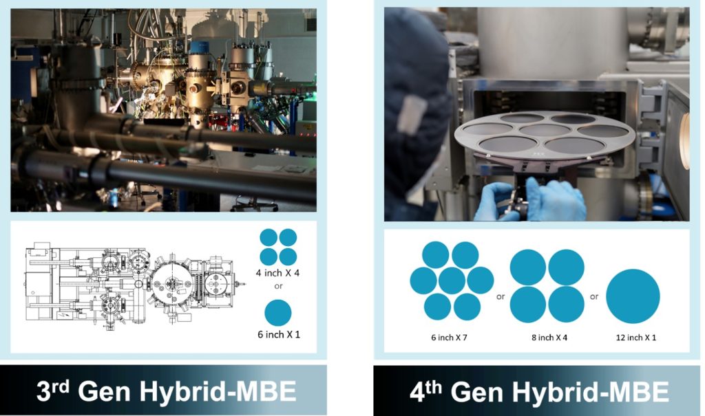
IVWorks grows n⁺-GaN using its proprietary Hybrid-MBE system. Now in its 4th generation, the Hybrid-MBE platform supports n⁺-GaN regrowth on wafers ranging from 2-inch to 12-inch diameters.
The Hybrid-MBE system developed by IVWorks is capable of using both N₂ plasma and NH₃ gas injection as nitrogen sources. Using N₂ plasma enables direct supply of atomic nitrogen, allowing precise control over the V/III ratio and minimizing hydrogen incorporation in the film, since no hydrogen byproducts are generated. However, due to the limited efficiency of atomic nitrogen generation, growth rates are relatively low, and it is challenging to ensure uniformity across large wafer areas.
In contrast, NH₃ gas injection allows for high-volume nitrogen delivery with excellent spatial uniformity, enabling faster growth rates under N-rich conditions and supporting uniform III-N film growth even on large-diameter wafers. One of the greatest advantages of NH₃-based growth in IVWorks’ Hybrid-MBE system is its ability to achieve perfect selective area growth.
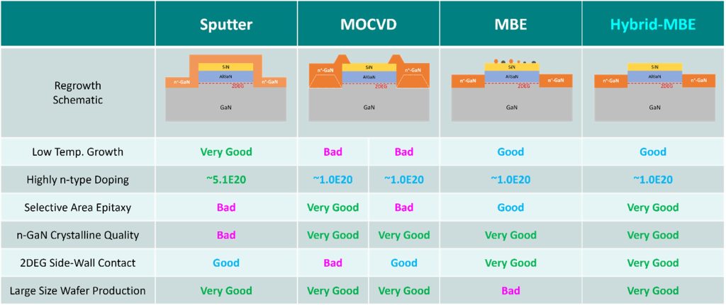
With perfect selective area growth of n⁺-GaN only in the Source/Drain regions, IVWorks’ Hybrid-MBE significantly simplifies downstream processing for customers—making it one of the most powerful and enabling technologies available.
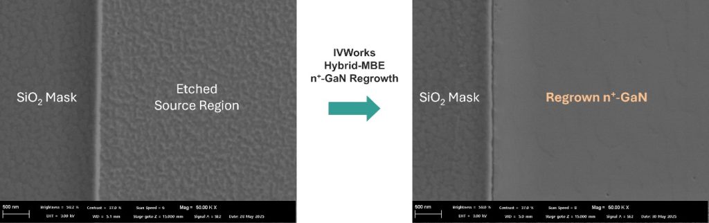
Although the etched regions of the patterned wafer provided by the customer were relatively rough, IVWorks successfully achieved perfect n⁺-GaN regrowth using its Hybrid-MBE and regrowth technology. Selective area growth was fully realized—no growth occurred on the mask regions, and n⁺-GaN was grown only in the Source/Drain areas. The regrown n⁺-GaN layer, precisely 80 nm thick, was grown in 2D mode, ensuring epitaxial contact with the 2DEG sidewalls.

To ensure uniformity, multiple locations across the 4-inch wafer—after n⁺-GaN regrowth—were precisely measured. With the results verified, we are now preparing the packaging for delivery to the customer.
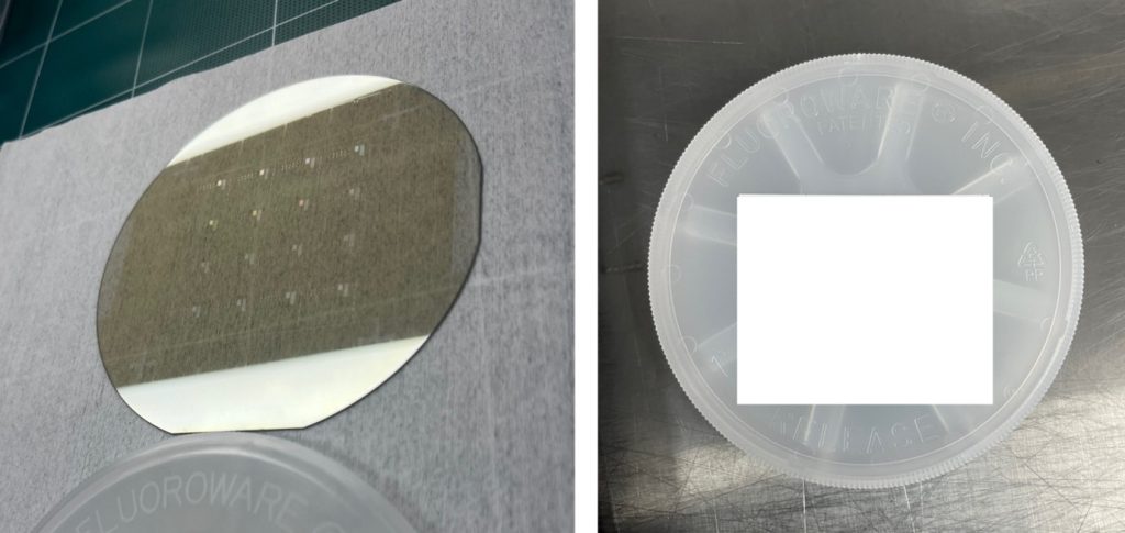
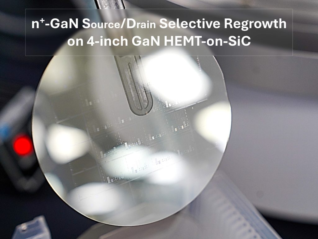
The 4-inch GaN HEMT on SiC wafer with n⁺-GaN selectively regrown in the Source/Drain regions has been vacuum-packed and shipped to the customer. IVWorks’ n⁺-GaN regrowth service supports wafer sizes from 2 inches to 12 inches, and is compatible with GaN HEMT structures on Si, SiC, and Sapphire.
Inquiries │IVWorks Website QNA or www.domm.ai/contact