media center

AlN HEMT on SiC Epiwafer
4, 6 inch by Hybrid-MBE
AlN HEMT Epiwafer?
<High Power RF Application>
· Large Bandgap AlN Buffer
· Higher Breakdown Field
· Outstanding Thermal Conductivity
· Stronger 2DEG Confinement Effect
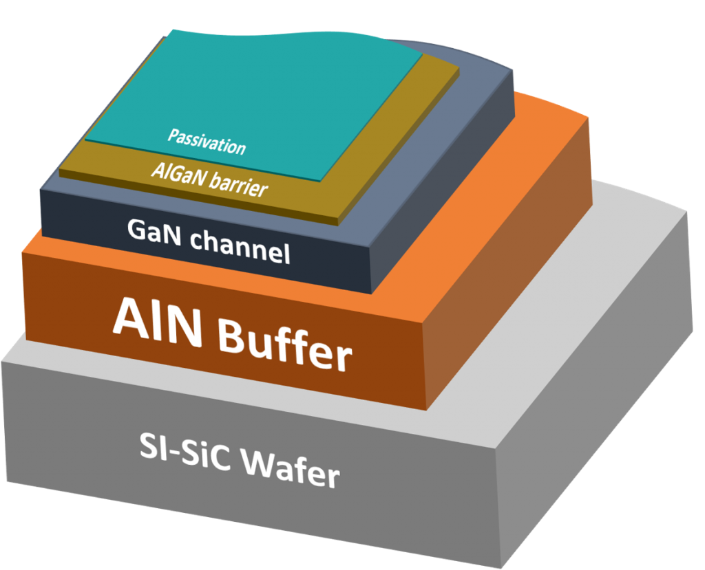
Product Structure
We are proud to unveil an innovative product after months of research, development and testing. And we’re happy to introduce this cutting-edge RF HEMT device material. Elevate your projects to new heights with our new GaN on SiC which is AlN HEMT Epiwafer.
| AlN HEMT Epiwafer | details |
|---|---|
| Cap | GaN 2㎚ or in- situ SiN 3 ㎚ |
| AlGaN Barrier | 18㎚ ~ 23㎚ / Al comp. 25% ~35% |
| GaN Channel | 350㎚ , 250㎚, 150㎚, 50㎚ |
| Undoped AlN Buffer | 700㎚ |
| Semi-insulating SiC | 4inch or 6inch / US or Non-US |
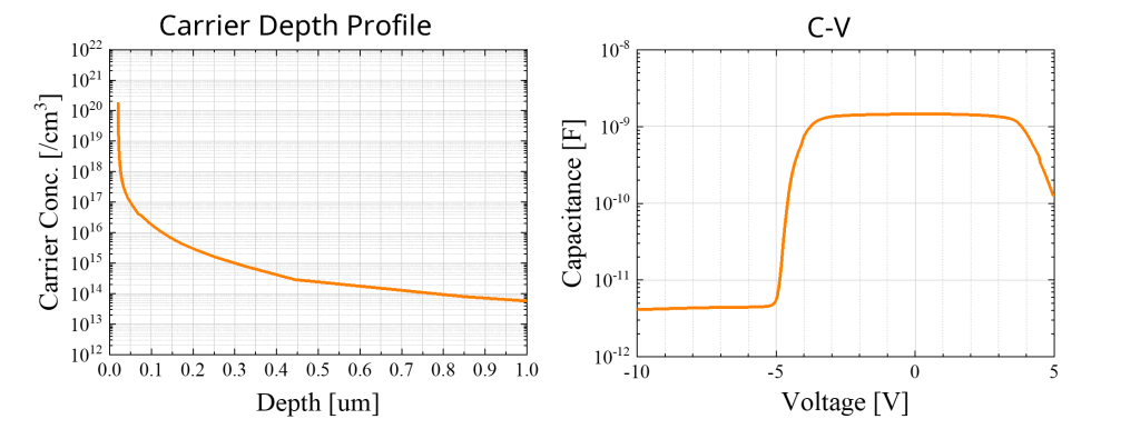
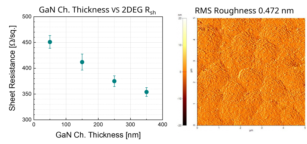
Product Specifications
· Wafer Bow : <30㎛
· Total Thickness Uniformity : <2%
· Edge Exclusion : 3㎜
· RMS Roughness : <1㎚
· 2DEG Rsh – GaN ch. 50㎚, 150㎚ : <470 Ω/sq. <Std. 3%
· 2DEG Rsh – GaN ch. 250㎚, 350㎚ : <400 Ω/sq. <Std. 3%
· Breakdown Voltage : >150V (1E-06 A/㎜)
What’s Properties?
What are the characteristic?
4th Generation Hybrid-MBE
Our newest product, the AlN HEMT Epiwafer is grown using IVWorks’ unique multi-wafer GaN MBE System. With a single growth process, it can produce 14 wafers of 4 inches, 7 wafers of 6 inches, 4 wafers of 8 inches.
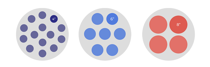
4 inch * 14 / 6 inch* 7 / 8 inch*4
Growth Monitoring using Artificial Intelligence Platform
The crystal structure information at the atomic layer level acquired in real-time is analyzed and applied using Artificial Intelligence by the RHEED monitoring technique of Hybrid-MBE to maximize yield rates.