
news
We have received a process order for n⁺-GaN regrowth from a company in the Asia region.
The patterned wafer provided by the customer is a 6-inch GaN HEMT on Si. RF GaN HEMT on Si technology is attracting strong market interest in relation to next-generation mobile communication applications. In particular, for mobile device applications, cost competitiveness is a fundamental requirement. Therefore, securing economic viability through a large-diameter wafer roadmap—from 6-inch to 8-inch to 12-inch—is essential, and GaN HEMT on Si plays a key role in enabling that transition.
Moreover, as the frequency bands of next-generation mobile communication are expected to integrate both the FR3 band (7–24 GHz) and satellite communication band (1–2 GHz), it becomes even more important to enhance performance and efficiency using GaN HEMT on Si technology. IVWorks’ n⁺-GaN regrowth process service supports not only 6-inch GaN HEMT on Si, but also 8-inch and 12-inch wafers. In addition, n⁺-GaN regrowth is available for various substrates including GaN on SiC, GaN on GaN, and GaN on Sapphire.
At IVWorks, n⁺-GaN is selectively grown only in the source/drain regions at a relatively low temperature of around 700°C. This enables non-annealed ohmic contact without the need for ohmic metal RTA, and allows contact resistivity to be easily reduced below 0.1 Ω·mm. This is a specialized epitaxy service unique to IVWorks. You can now design a wide range of epitaxial structures—including n⁺-GaN regrowth and p-GaN regrowth—and get instant quotes in real time at domm.ai/epidesign.
At IVWorks, when we receive patterned wafers from customers, the first step is to inspect the etched surfaces of the Source/Drain regions—where selective regrowth will take place—using SEM measurements.
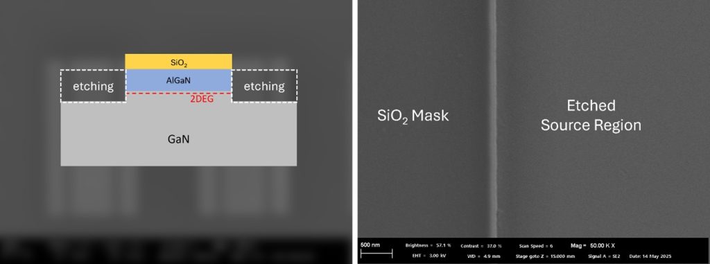
The patterned wafers we received for this order used SiO₂ as the mask material. Both SiO₂ and SiN are ideal mask materials for IVWorks’ selective area regrowth process—no growth occurs on the masked regions, and n⁺-GaN is grown exclusively in the Source/Drain areas.
The patterned wafer provided by this customer, as expected from a high-volume production company, had a very clean etched surface in the source/drain regions. As mentioned in our previous post, etching processes vary by customer, so the surface conditions after etching can differ case by case. In particular, compared to production companies, etched surfaces from research institutes or university labs tend to be rougher and less uniform. To address this, IVWorks applies initial growth conditions that maximize surface recovery at the beginning of the regrowth process, minimizing the impact of etching surface variation. Based on our experience, as long as there is no residual mask material (such as SiO₂ or SiN) left on the etched surface, recovery is usually achievable.
So don’t hesitate to try n⁺-GaN regrowth, even if your etching process is not yet fully optimized.
At IVWorks, before performing n⁺-GaN regrowth on customer wafers, we first grow an n-GaN test wafer under the exact same growth conditions intended for the regrowth process. This test is conducted on a wafer that matches the customer’s in material and wafer size, allowing us to verify the n-type doping conditions in advance. By doing so, we ensure high process accuracy and consistency for the final regrowth on the customer wafer.
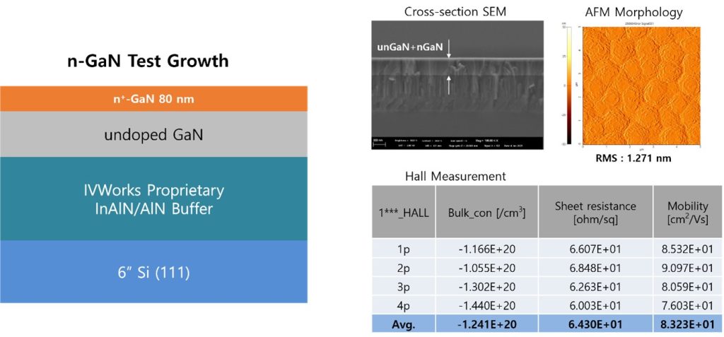
For this project, we grew an n-GaN test structure on a 6-inch Si(111) wafer, identical to the patterned wafer provided by the customer.
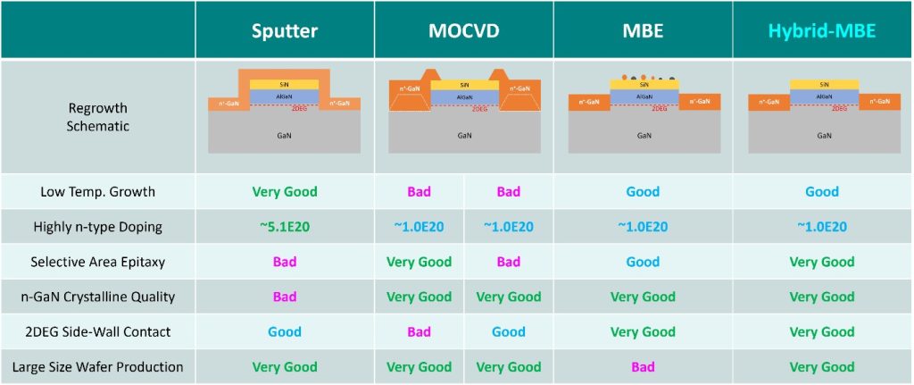
Growing GaN on Si wafers is significantly more challenging than on other substrates such as SiC, Sapphire, or free-standing GaN. It requires overcoming lattice mismatch and crystal structure differences between the Si substrate and the III-nitride films, while precisely managing thermal expansion mismatch, film stress, and maintaining insulating properties of the buffer layers. Additionally, since direct contact between gallium and the silicon wafer can lead to melt-back etching, special care must be taken to prevent gallium exposure to the Si surface during growth.
IVWorks provides a GaN on Si epitaxy platform using its proprietary patented InAlN/AlN superlattice buffer technology. The InAlN/AlN superlattice buffer maintains a high superlattice bandgap energy to enhance insulating properties, while leveraging the lattice mismatch between InAlN and AlN to precisely control film stress.
This technology can be flexibly applied to both RF GaN HEMT on Si and DC power GaN HEMT on Si epiwafer structures.
Following the growth of the n-GaN test structure, we confirmed the exact growth rate and n-type doping characteristics. With an n-doping concentration of 1.24e20 cm⁻³, sufficient doping was verified, and growth on the customer’s patterned wafer will proceed under the same conditions.
IVWorks grows n⁺-GaN using its proprietary Hybrid-MBE system, developed in-house.
Currently in its 4th generation, the Hybrid-MBE platform supports n⁺-GaN regrowth on wafers ranging from 2-inch, 4-inch, 6-inch, and 8-inch up to 12-inch in diameter. For an introduction to Hybrid-MBE, please refer to: 4″ GaN HEMT with n⁺-GaN S/D Selective Regrowth for Asian University
IVWorks’ Hybrid-MBE operates under Level 4 of Domm-ai, our proprietary AI agent system, which enables autonomous production through Automation, Monitoring, Real-time Pass/Fail Prediction, and Alerting.
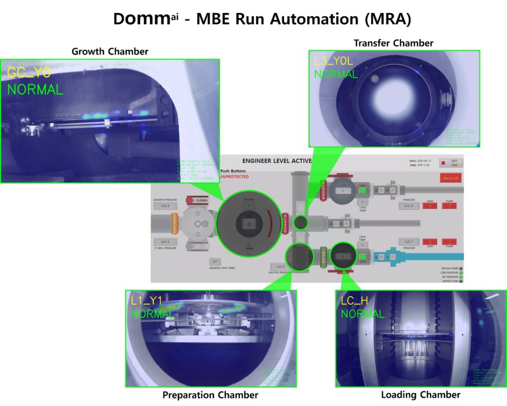
To enable continuous production without the presence of an operator, the Loading–Growing–Unloading sequence of the wafer is managed by our MBE Run Automation (MRA) system, which is trained through machine learning. Throughout the entire epitaxial growth process, the electron diffraction patterns of the crystal growth surface are analyzed in real time, and a Pass/Fail prediction model is used to continuously score the epiwafer quality.
If the probability of passing quality standards drops, or if anomalies are predicted in parameters such as vacuum level, source cell temperature, manipulator temperature, or various sensor readings of the Hybrid-MBE, the system immediately issues an instant notification to the engineer and triggers feedback actions accordingly.
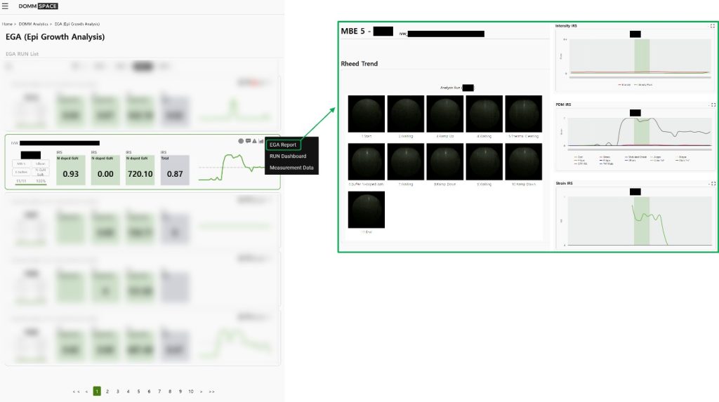
In this n⁺-GaN regrowth, the wafer was patterned with a SiO₂ mask, so the electron diffraction pattern appeared relatively weak. However, it was still sufficient for Domm-ai to perform real-time analysis. Throughout the entire growth process, Domm-ai continuously analyzed the intensity of the electron diffraction pattern, the growth mode (PDM) transitions, and strain variations in real time. Based on this analysis, the system predicted the wafer quality and ultimately recorded a high score of 0.87. Even from Domm’s prediction result alone, it was evident that the selective area growth of n⁺-GaN was successfully completed, and that n⁺-GaN was grown in a 2D mode.
IVWorks leverages its proprietary Hybrid-MBE technology to achieve perfect selective area growth of n⁺-GaN exclusively in the source/drain regions, while maximizing productivity through the Domm-ai system.
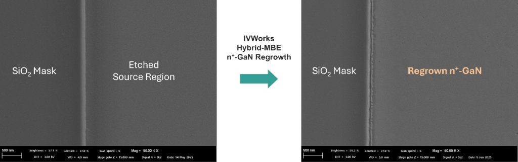
The n⁺-GaN regrowth requested by the customer was successfully completed using IVWorks’ Hybrid-MBE and regrowth technology. Perfect selective area growth was achieved, with no growth observed on the masked regions, and n⁺-GaN was grown only in the source/drain regions to a target thickness of 80㎚, maintaining 2D-mode growth for proper epitaxial contact with the 2DEG sidewalls. Even on the fine steps formed at the interface between the SiO₂ mask and the etched regions, the n⁺-GaN layer grew smoothly and uniformly, ensuring complete coverage.

To ensure uniform n⁺-GaN regrowth across the full 6-inch wafer, multiple locations on the wafer were precisely measured by position. We are now preparing packaging for delivery to the customer, following this verification.
The wafer, with n⁺-GaN selectively regrown in the source/drain regions of a 6-inch GaN HEMT on Si, has been vacuum sealed and successfully shipped to the customer. IVWorks’ n⁺-GaN regrowth service supports wafer sizes from 2 inches to 12 inches, and is compatible with GaN HEMT structures on Si, SiC, GaN and Sapphire.
Inquiries │IVWorks Website QNA or www.domm.ai/contact