
news
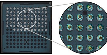
Series 1. image data in angstrom unit
IVWorks combines epitaxy technology with artificial intelligence (AI) to provide differentiated, high-quality Epi wafer foundry services. Three articles are presented in this series in which we divide semiconductor manufacturing and AI series into data, model, and platform, respectively. Let us explore the appearance of a semiconductor from the perspective of a researcher directly involved in DOMM AI Epitaxy System research.
Numerous semiconductor manufacturing processes are required when producing semiconductor products. Depending on its purpose, a unit product is developed by applying the most suitable processes, such as epitaxy, etching, impurity injection, and light exposure, to the mother substrate. Once the manufacturing process is complete, the product should undergo the packaging process to protect the semiconductor from external environment before it can be released to the market. These semiconductor components are widely used in various fields, such as 5G mobile communication, military radar, electric vehicles, and Internet of Things (IoT).

The semiconductor manufacturing field is transforming toward the “AI Factory” implementation over simple automation to take the lead in the development of higher-quality semiconductor structures. Thus, transmission, management, and application of various sensing data (such as temperature, amount of control gas, mechanical movement), which are combined with vision data and IoT, are crucial.
Prior to this, IVWorks has developed the world’s first AI epitaxy platform, DOMMTM, which combines the AI technology with the epiwafer production. IVWorks offers distinguished epiwafer foundry services with its advanced automated system such as DOMMTM.
In this article, we will learn about the image data obtained from our epitaxy system, as well as those for utilizing AI in the processes of semiconductor fabrication.
“How do semiconductor manufacturers use deep-learning image analysis?”
Nowadays, semiconductor manufacturing companies are applying deep learning approaches on images to improve the process of detection of defects that are difficult for humans to distinguish. The “VisionPro” inspection equipment from the United States can detect wafer defects as small as 15 μm, and the ‘Cognex’ equipment is used for solar panel inspection to detect various mechanical errors. Further, the Ball Grid Array (BGA) vision inspection system of TT Vision in Malaysia has an accuracy of 17 μm for 0.2 mm balls and a fast inspection time of about 180 ms. However, as mentioned previously, the deep-learning analysis using images in the field of semiconductor manufacturing is limited to the back-end processes.
Numerous physical and chemical changes occur during the manufacturing process of compound semiconductor, which must be observed and controlled in real time. Many parameters must be considered for control, and the product quality highly depends on the skill level of the engineers.
The purpose of using the AI technology is to overcome the limitations of decision making based on experiences and intuition of professional personnel and to develop high-quality semiconductor structures through data-driven decision-making process. Therefore, high-quality data are essential for the effective application of an artificial intelligence model. IVWorks obtains high-quality image data during the fabrication process of compound semiconductor devices.
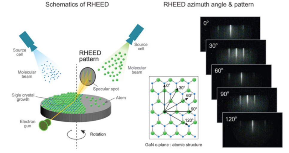
Reflection high-energy electron diffraction (RHEED) refers to a technique used to characterize a pattern that appears on the fluorescent screen by an electron beam incident at a glancing angle of 1°~5° on the substrate (sample) surface during the manufacturing process. This technique also enables real-time image analysis. Using reflection and diffraction properties, changes in the atomic spacing [lattice constants : GaN (a = 3.189 Å), AlN (a = 3.112 Å), InN (a = 3.544 Å)] of the compound semiconductors at sub-angstrom (10-10 m or below) level [1] could become visible on the fluorescent screen, which are observed and collected.
In general, a compound semiconductor device has a heterostructure. The quality (crystallinity, roughness, interface abruptness, strain, etc.) and performance (electron mobility, sheet resistance, etc.) of a compound semiconductor device depend on how precise the process controls the degree of change in the atomic lattice structure generated during the stacking of materials with different physical and chemical properties, as well as the thermal expansion coefficients.
Further, the degree of change can only be adjusted by observing the change at sub-angstrom level, as mentioned previously. In addition to the lattice constant, DOMMTM enables observation of changes in various patterns according to the production conditions and helps learn, predict, and apply the image information to the production process.
Image data are the most complex data type that can be learned and utilized effectively in artificial intelligence and, thus, are used in various manufacturing fields. However, not all manufacturing processes can offer high-quality data. In particular, IVWorks has the optimal manufacturing process that can employ artificial intelligence. Therefore, we are confident that we will pioneer the core field of artificial intelligence manufacturing technology in the future.
[1] length unit: millimeter (mm, 10-3 m), micrometer (μm, 10-6 m), nanometer (nm, 10-9 m), angstrom (Å, 10-10 m)
Byung-Guon Park / Artificial Intelligence team