
news
How AI-Agents Are Transforming the Materials Ecosystem, Part 2: From Lab to Mass Production
Editor’s Note:
This post is the second part of the three‑part series titled “How AI‑Agents Are Transforming the Materials Ecosystem.” In the previous article, we introduced the basic concept of AI‑Agents and discussed why semiconductor materials companies are looking to build them. In this second installment, we focus on epitaxial wafer production examining AI‑Agents from a manufacturing perspective and how they are being applied. As before, this series emphasizes insights over technical detail, serving as a primer to help you better understand future technical columns. Please feel free to comment with any questions. We appreciate your interest in IVWorks’ AI research!
Traditional Epitaxy Methods and Their Limitations
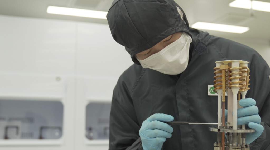
Epitaxial growth, a process considered the most critical step in securing a stable supply of gallium nitride semiconductors, involves layering extremely thin films on a substrate at the atomic level. This is an extremely delicate and complex procedure, as it requires nanometer-level precision in controlling physical reactions that occur under high-temperature and high-vacuum conditions. Despite its sophistication, the traditional methods of epitaxial growth that have been used until now reveal several limitations. These are not necessarily technical flaws, but rather commercial constraints that become evident in mass production environments.
A Slow Cycle for Quality Improvement
◇ Immediate decisions and interventions to prevent process risks
Epitaxy is inherently unsuitable for parallel experimentation. Typically, it follows a cycle of ‘growth → condition adjustment → regrowth’. If the measurement results of the grown wafer fall short of the target, parameters such as flux, temperature, doping concentration, and growth rate are adjusted, and the growth process is repeated. This cycle is repeated multiple times until the desired epitaxial structure is achieved—a method that has long been used in both research and industrial settings.
At first glance, waiting for potentially defective wafers to finish growing might seem inefficient. Depending on the method used (MBE, MOCVD, HVPE, etc.), epitaxy is typically conducted in sealed environments. Since it’s difficult to visually inspect progress during the process and not feasible to test multiple conditions simultaneously due to equipment constraints, the only viable strategy is to finely tune and verify each condition through repeated trials.
However, this also means that improvement cycles are slow, and process optimization often depends heavily on the engineer’s experience and intuition. While some tools like RHEED, reflectometry, or pyrometers, do allow partial real-time monitoring, interpreting these signals still requires human judgment. Whether a signal variation indicates an anomaly or falls within acceptable bounds is ultimately a subjective call. As a result, different engineers may interpret the same data differently, and crucial signals can sometimes be overlooked. This makes real-time error detection during growth difficult, and in most cases, issues with process conditions are only recognized after the run is complete.
◇ High Experimental Costs Due to Repeated Cycles
Because parallel experimentation is structurally difficult and continuous human oversight is required, each experimental run demands significant time and resources. When accounting for setup, parameter adjustment, processing, post-treatment, and analysis, even a single cycle can take several hours or even dozens of hours. As the number of iterations increases, the cumulative cost in both time and money becomes substantial. In real-world production settings, it is not feasible to repeat such experiments indefinitely. This ultimately places constraints on manufacturing throughput.
Challenges in Reproducibility and Consistency
◇ A Process Without a Clear “Correct” Answer
Another key challenge of epitaxial growth lies in its numerous variables, which are often nonlinearly interrelated. This makes it nearly impossible to pre-calculate the exact optimal conditions. Typically, parameters are set based on expert experience and historical data. However, even with identical settings, outcomes may vary due to changes in equipment condition or environmental factors. In such uncertain and complex scenarios, it’s difficult to reliably identify optimal conditions using traditional experimental methods alone. In mass production, reproducibility and consistency of process conditions are critical. While it may be possible to achieve a certain quality level in small-scale experiments, replicating the same results reliably in a full-scale production environment is a far more challenging task.

Why Should We Address These Limitations?
The compound semiconductor industry has not yet reached maturity. Unlike silicon-based semiconductors, compound semiconductors such as GaN and InP have a relatively short commercial history, and both the technology and its ecosystem are evolving rapidly. This means that companies able to establish a technological edge early on are far more likely to dominate the market in the long term.
However, quality alone is not enough.
A certain level of quality is now considered a basic, non-negotiable requirement in the market. Customers increasingly prefer partners who can not only maintain high quality but also offer shorter lead times and greater flexibility in delivering custom specifications. Due to the complex composition and intricate processing of compound semiconductors, there is significant pressure to achieve maximum results from each experiment and production run. As market trends sift rapidly and development speed itself is now seen as a key competitive edge, failing to eliminate inefficiencies in this changing environment will inevitably lead to falling behind in the competition.
The problem is that traditional production methods alone are no longer sufficient to meet these demands.
In manufacturing, cost and time are crucial. As we’ve seen earlier, the traditional approach of optimizing process conditions one by one through experimentation is costly and time consuming, making it difficult to respond quickly maintain consistent quality. Moreover, relying solely on engineers’ experience to predict and reproduce the complex interactions among dozens of variables is increasingly unrealistic. These limitations stand in direct conflict with evolving market expectations.
This is why IVWorks is striving to gain a technological edge through the automation and intelligent transformation of epitaxial growth processes. The goal goes beyond simply replacing human labor with AI. What’s needed is a system that can reliably analyze processes based on data, predict potential failures in advance, learn the complex interdependencies among variables, and propose or adjust optimal epitaxy conditions autonomously. The AI-based epitaxial process innovation led by IVWorks has now attracted the attention of latecomer companies. But IVWorks’ automation efforts are not merely aimed at operational efficiency—they serve as critical technological infrastructure for solidifying a leadership position in the GaN market, where neither industry standards nor market dominance have yet been clearly established.
Reflecting on the limitations discussed above, several natural questions arise:
‘Is there a way to accelerate the improvement cycle?‘
‘Can we grow high-quality epitaxial layers from the start, without needing to adjust conditions later?‘
‘Is it possible to dramatically improve productivity?‘
‘What if engineers didn’t need to be constantly monitoring equipment? What if human error could be minimized? What if optimal growth conditions could be pre-calculated?‘
If ideas like these can be realized, it would open a path toward overcoming the fundamental structural constraints of epitaxial processing.
Case Study: Optimizing Epitaxy Productivity with AI Agents
In a previous article, we introduced IVWorks’ AI Agent as a concept that integrates and expands various automation elements required for epitaxial growth. Today, we’ll take a closer look at one of its core components: MRA (MBE Run Automation). Planned by a task force composed of AI engineers and epitaxy specialists last year, MRA has recently begun implementation on real production lines. This project literally means “run automation,” that is, an unmanned autonomous production system where AI independently operates the MBE epitaxial growth process.
The key concept is “human absence.”
Epitaxial growth continues without requiring an engineer to be physically present. Let’s explore what that actually means.
Human Intervention in Epitaxy: Still Essential
◇ Real-Time Decisions and Intervention to Mitigate Process Risks
To produce high-quality epitaxial wafers, various parameters across multiple stages, from wafer loading and vacuum creation to run readiness, growth, and cooling must be managed and adjusted in a timely manner. In the past, operators had to manually press “Start” at each step. Today, built-in software automates the sequence, allowing the process to progress on its own. However, this automation follows only a predefined mechanical flow and cannot respond to real-time issues such as physical anomalies or system errors.
When unexpected changes occur, such as vacuum fluctuations, equipment malfunctions, or temperature variations, real-time judgment and response are needed. In such cases, human intervention becomes necessary. That’s why, traditionally, engineers have always had to be present during the epitaxial process.
Let’s take the “wafer loading issue” as an example.
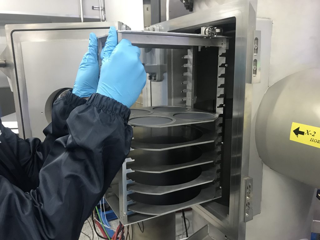
The first step in epitaxy is to place the wafer holder into the loading chamber. In an MBE system, multiple chambers are connected, and a robotic arm transports the holder between them. But what happens if the holder is slightly misaligned? It may collide with internal components during transfer or cause the wafer to tilt and crack.
Loading errors can occur for a variety of reasons.
These include wafer contamination, holder wear, coordinate misalignment, and systemic factors like temperature gradients or vibrations inside the equipment. Errors can also stem from initial setup issues or physical misalignments. Such loading problems can lead to compositional imbalances, crystal defects, or complete growth failures, making it difficult to produce high-quality wafers.
What’s more, these issues can cause significant system-level losses. For example, if a holder is dropped inside the chamber, the vacuum that has been built up over several hours must be broken to recover it. This triggers a time-consuming recovery process, often requiring source re-deposition and delaying the entire production schedule by more than a week. Beyond material costs, the indirect losses from disrupted production are substantial. To avoid such risks, engineers have traditionally monitored equipment continuously during each run, responding immediately to any signs of abnormality.
And this issue is not limited to the loading stage alone.
During thin-film growth, real-time responses to a wide range of variables are also essential. These include maintaining and adjusting growth conditions, detecting crystal states via RHEED patterns, determining whether to halt the process when vacuum gauge warnings occur, and stabilizing cell temperatures. Because such decisions require quick and accurate responses, engineers have historically been unable to leave the production line unattended during epitaxial growth.
◇ What changes with MRA?
The image below shows a wafer holder being loaded into the chamber. MRA continuously analyzes the movements of both the wafer and holder in real time and calculates an anomaly prediction score, a numerical representation of how much the current state deviates from the normal. The AI model learns from historical process data and equipment behavior patterns, then compares them against real-time movement. If current behavior strays outside the expected range, MRA instantly detects the abnormality (as seen in the “abnormal” state on the right).
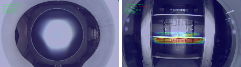
In such cases, MRA can autonomously halt the task based on its own judgment. Depending on the situation, it may also prompt the operator with a set of options and request a new task. Every event and action that occurs during the process is communicated to the engineer in the form of a message. These messages include real-time process footage along with explanations of the detected risks and the system’s corresponding responses. This means engineers no longer have to physically stand next to the machine to oversee the process. They can remotely monitor the wafer loading stage and remain fully informed about the status of the run without missing any critical information.
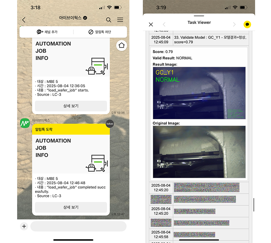
MRA operates reliably even during nights and weekends when no operators are on site. Individual process steps, including wafer loading, can be scheduled for automatic execution. Operators can predefine the sequence and timing of tasks in advance, allowing processes to run unattended outside of regular working hours. This resolves a major limitation of traditional methods, where processes were constrained by operator availability. Now, production can continue reliably even during off-hours, contributing significantly to improved productivity. This system is already in full operation at IVWorks’ fabrication facility.
For foundries, where mass production and sales are the ultimate goals, productivity is a critical factor. Companies must complete as many meaningful runs as possible within limited working hours. In this context, MRA not only ensures consistent quality but also enables the production of more high-quality wafers within the same time frame.
Although we’ve focused on a single use case here, MRA functions as if a highly experienced engineer were monitoring the production line 24/7. It detects abnormalities at every stage in real time, makes appropriate judgments based on the situation, and can even notify the operator or present response options when necessary. This represents more than just automation—it’s a shift toward autonomous processing, where the system can perceive, decide, and act on its own.
Today, we’ve explored the limitations of traditional epitaxial methods and introduced a small-scale application of MRA as a solution for improving production in mass manufacturing environments. In the next installment of this series, we’ll take a closer look at how IVWorks is concretely addressing the ideas and challenges that emerged from those limitations.
Yoon-Seo Cho l Marketing Manager t at IVWorks
※This article reflects the subjective opinions of the contributor and may differ from the official position of IVWorks