
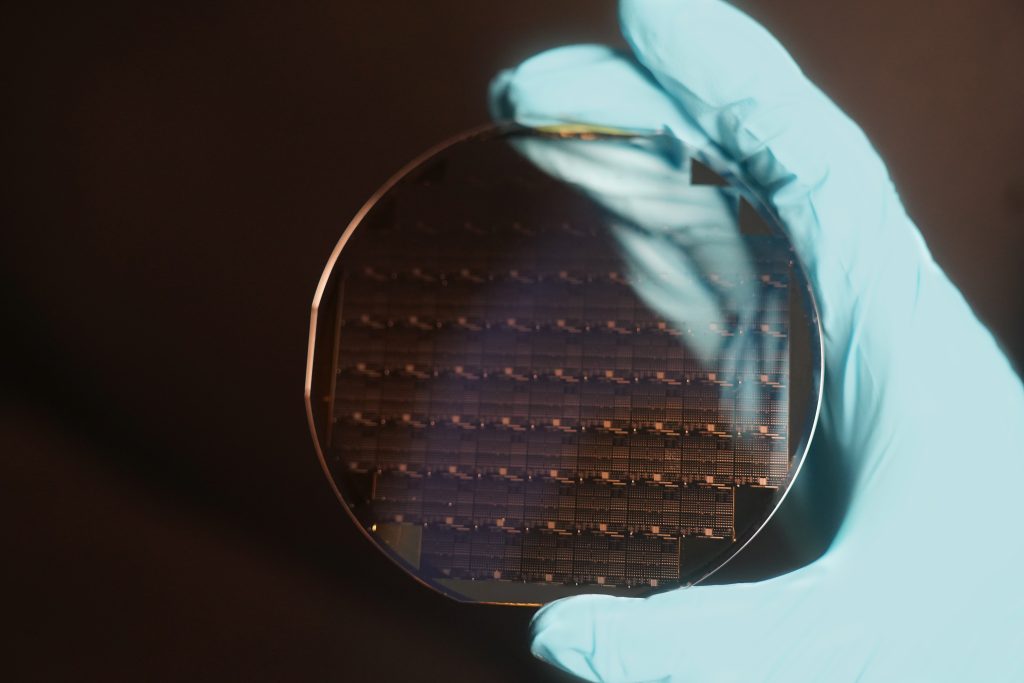
news
“IVWorks, Maximizing device performance by lowering contact resistance and improving electrical properties through n+-GaN selective regrowth”
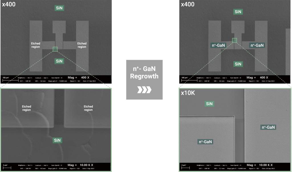
In September last year, IVWorks introduced the industry’s first n+-GaN Selective Regrowth service utilizing MBE (Molecular Beam Epitaxy) equipment. This service selectively etches the source and drain areas of GaN epi-wafers. It then precisely regrows n+-GaN to reduce contact resistance, enhance electrical properties, and improve semiconductor device performance.
High temperatures during the regrowth process can degrade the quality of the epi-interface, adversely affecting device performance. IVWorks’ Hybrid-MBE process operates in an ultra-high vacuum with minimal impurities. It enables low-temperature processing below 700°C. Additionally, in-situ surface cleaning technology removes impurities from the wafer surface, preventing HEMT device performance degradation during the regrowth process.
| Contact Resistance : Achieves levels as low as ≤ 0.1 Ωmm | |
| Uniformity : 2% or less | |
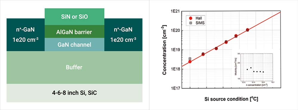
| High Doping Concentration (n=5.0e19 ~ 2.0e20/cm3) | |
| 2DEG Side-Wall Contact with Regrowth n+GaN Epitaxially | |
| Processing Time : Approximately 2 hours |
Thanks to these technical advantages, IVWorks’ Regrowth service offers exceptional precision and reproducibility in semiconductor device manufacturing.
The n+-GaN Selective Regrowth technology significantly reduces ohmic contact resistance. Resistance can drop to as low as 1/10 of conventional levels, offering superior performance. This reduction minimizes resistance during current flow, significantly decreasing power loss and maximizing device efficiency. Such improvements play a vital role in enabling high-performance device designs and miniaturization.
In particular When applied to RF devices, this technology significantly enhances power efficiency and density. It is particularly valuable in high-frequency environments requiring stable signal processing.
IVWorks’ Regrowth service is compatible with 4-inch, 6-inch, and 8-inch silicon (Si) substrates, as well as 4-inch and 6-inch silicon carbide (SiC) substrates. Its excellent performance has been consistently proven through customer applications. It is highly trusted by leading global semiconductor companies and research institutions.
In February, IVWorks further expanded its offerings by launching the p-GaN Gate Selective Regrowth technology, providing customers with an even broader range of options and reinforcing its technological leadership.
IVWorks’ Selective Regrowth service is available on the WIZDOMM platform (▶https://www.domm.ai/epidesign). Customers can adjust etch depth and mask parameters to design optimized processes. The platform provides instant quotations, saving both time and cost.
Experience the cutting-edge Regrowth technology from IVWorks!
Soo-Jeong Choe l Marketing Assistant Manager at IVWorks
※This article reflects the subjective opinions of the contributor and may differ from the official position of IVWorks