
news
Series 1. Machine learning for image analysis
IVWorks combines epitaxy technology with artificial intelligence (AI) to provide differentiated, high-quality Epi wafer foundry services. Three articles are presented in this series in which we divide semiconductor manufacturing and AI series into data, model, and platform, respectively. Let us explore the appearance of a semiconductor from the perspective of a researcher directly involved in DOMM AI Epitaxy System research.
Artificial intelligence (AI) has become an intrinsic part of our daily life. Various industries, including semiconductors, are trying to introduce AI technology to collect data worldwide, from numerical to image and voice data, to create new services. Among the various types of AI technologies that enrich our lives, we will examine AI algorithms and trends that use images.

“When image analysis is used well…”
Image deep learning technologies commonly used in the industry include classification, object detection, and semantic segmentation. In classification, a machine learning algorithm assigns labels to a number of existing images previously collected from a database and continues learning them to accurately classify new images according to the labels. The scenario with the wine from the previous paragraph is an example of classification, in which the AI provides information classified based on the previously learned image labels.
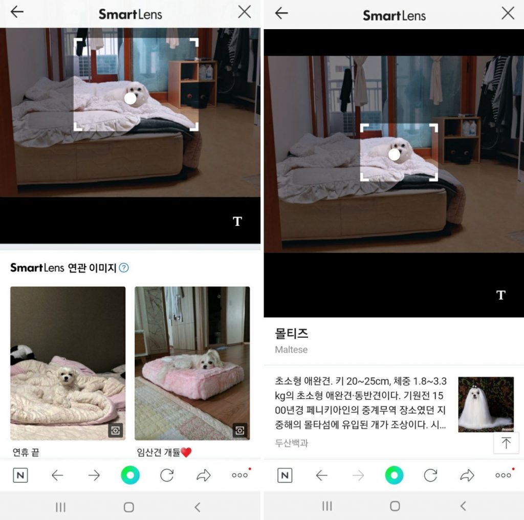
NAVER utilizes the classification technology in its app, ‘SmartLens’. When SmartLens captures a photo or loads a photo from the album, it recognizes the image and finds similar images. For example, if the image has an animal or a flower, it retrieves information such as species or breed from encyclopedias. From a human face, it can determine the age, facial expression, and celebrities that the person looks like using facial recognition.
In object recognition, several objects are identified from a single image. The difference from classification is that several classes exist in one image. Hence, 1) it first determines the object’s location in the image (bounding box), and then 2) the classification algorithm is used within the bounding box. An algorithm used in autonomous vehicles is a prime example of object recognition technology.
[1] NVIDIA, a leader in the field of autonomous vehicle research, unveiled the next-generation autonomous driving platform, NVIDIA DRIVE AGX Orin, at GTC China in December 2019. Orin is designed to manage numerous applications and deep neural networks that work simultaneously on autonomous vehicles and robots while meeting systematic safety standards such as ISO 26262 ASIL-D. The object recognition technology detects lanes, road markings, and even vertical landmarks, whereas semantic segmentation technology enables the recognition of the surrounding environment in detail, subdividing it in pixel levels for precise results.
[1] Resource : NVIDIA https://blogs.nvidia.co.kr/2019/12/19/orin/
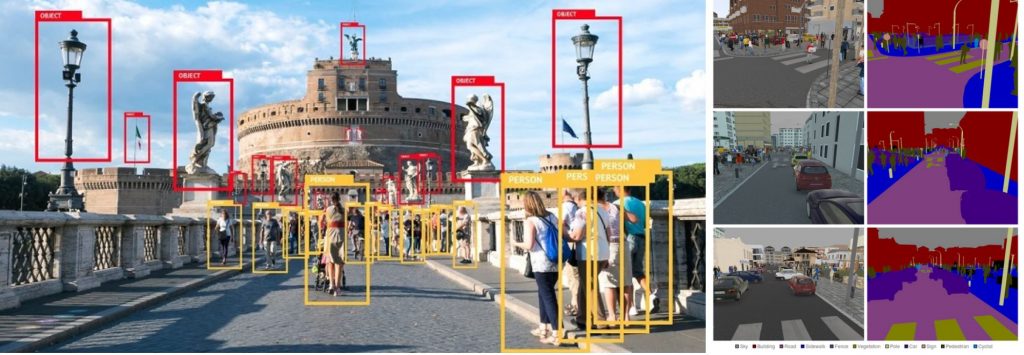
Unlike object recognition, semantic segmentation performs image labeling at each pixels. The goal is to accurately distinguish the boundaries of images. This algorithm is often used in medical images (X-ray, CT, etc.) because it subdivides an image into smaller parts that are difficult for humans to distinguish.
Using these AI algorithms enables automation of industrial equipment and robots, and delivers significantly precise results.
“Using an image analysis model in the industrial field”
AI first attracted attention with the image analysis model, which boasts high performance and rapid development among various AI models, even surprising the research team. New AI algorithms are being developed constantly, and it is easy to implement and employ the latest algorithms.
As deep learning-based image analysis models are being applied to various industries, one may expect to see better results. However, only a limited number of industries are able to apply image analysis models without difficulty. The application of AI in industrial fields is considerably different from commonly used image deep learning technology. Therefore, the following aspects should be considered.
· The first aspect is gaining a deeper understanding of research regarding AI. AI models are not universal. All members at a workplace should have a clear understanding of the purpose and use of AI for the desired outcome. Additionally, it is dangerous to assume that AI will do everything for you. This perception is risky for any company. The extent, level, and duration of work for the AI model should be clearly set for each task.
· The second aspect to consider is data. Users should be aware of what data are available and how they can be used. In most industries, one might assume that they have a considerable amount of data, but it might be different for AI. Data are the most important and difficult aspect of applying an AI model. The importance of data can be overlooked, as online class or schools regarding to AI often use publicly available datasets. Therefore, the following questions should be asked prior to the application of AI: ‘Are there any data that fit the job? If so, how will they be collected and processed?’ Sometimes people produce fake data or create data by rotating or manipulating an image, but these are not essential.
· The third aspect is determining an AI algorithm that can achieve the above goals quickly and flexible. However, numerous AI algorithms exist. In particular, there are many algorithms used for image analysis, and their performance is gradually improving due to many researchers’ efforts. It is important to apply a model that is appropriate for the task. Selecting the appropriate resolution, speed, and accuracy should precede tuning.
The Artificial Intelligence Research Team and the Epitaxy Team of IVWorks have a high-level of understanding of the semiconductor industry and clear goals for the mass production products. The reflection high-energy electron diffraction (RHEED, an image that appears on a fluorescent screen when an electron beam irradiates the surface of a substrate (sample)) image data generated during the production of an epiwafer have varying physical and chemical properties.
In addition, various analyses are performed with a system (AI epitaxy platform DOMM™) that enables the collection, processing, model learning, and real-time operation of the forecasted model of all epi layer growth structure data.
The analysis to get our goal requires more than simple image analysis algorithm. Moreover, analysis of the sequence of images over time series, or videos, is essential. To utilize image analysis, various factors must be considered. The next article will introduce an AI model that combines several models including a video analysis model as an ensemble for effective AI model application.
Seul-Lam Kim l Artificial Intelligence team